Spread spectrum clock generator and integrated circuit device using the spread spectrum clock generators

a technology of spread spectrum clock and integrated circuit, which is applied in the field of circuitry, can solve the problems of insufficient methods for effectively reducing electro magnetic interference, insufficient noise reduction of digital circuit, and insufficient reduction of magnetic interference components and jitters, so as to suppress the occurrence of additional emi components, prevent precipitous phase variations, and high precision

Active Publication Date: 2005-01-13
RENESAS ELECTRONICS CORP
View PDF11 Cites 49 Cited by
  • Summary
  • Abstract
  • Description
  • Claims
  • Application Information

AI Technical Summary

Benefits of technology

The spread spectrum clock generator of the present invention prevents precipitous phase variations in the output high frequency clock fo and can suppress the occurrence of additional EMI components due to phase jump.
The spread spectrum clock generator of the present invention can be configured without using an analog modulator and a highly precise sine wave generator and can easily be integrated into a semiconductor chip in which relatively large digital circuits are integrated like a microprocessor. Accordingly, micro ICs as shown in FIG. 13 can be realized with the above clock generator and, in its possible application, a great number of sensors may be networked.
FIGS. 19 through 21 show results of spectrum analysis obtained by simulating the performance of the spread spectrum clock generator of the present invention. FIG. 19 shows the result of spectrum analysis for the clock generator employing a so-called “PN9” random signal generator; FIG. 20 shows the result of spectrum analysis for the clock generator employing a triangle wave signal generator; and FIG. 21 shows the result of spectrum analysis for the clock generator employing a sine wave signal generator.
In FIGS. 19 through 21, there are shown the results of two cases: (I) spectrum is spread; and (II) spectrum is not spread. In these figures, the abscissa indicates signal frequency f [GHz] and the ordinate indicates output signal level [dBm]. Conditions of simulation: spread frequency width is 30 kHz and oscillation frequency is 1. 5 GHz. As is apparent from these figures, PN9 results in the most reduction in output level for spread frequencies, the triangle wave is the next, and the sine wave is the third. For the sine wave, the output level slightly rises at the edges of the spreading band, but has the EMI reduction effect as well as the PN9 and triangle wave.
The spread spectrum clock generator of the present invention can be configured as a two-point modulation, spread spectrum clock generator like configuration examples shown in FIGS. 14 and 15. Thereby, it is possible to more broaden the frequency band width of a modulating signal for spread spectrum implementation and thus the EMI reduction effect can be enhanced more.

Problems solved by technology

However, these methods are regarded as insufficient in effectively reducing the Electro Magnetic Interference, because the following problems are not well taken into consideration.
Such a phase jump gives rise to additional Electro Magnetic Interference components and jitters, which poses a problem.
Second, the above methods are vulnerable to noise produced from digital circuits.
However, if the above clock generator is realized on a semiconductor chip in which relatively large digital circuits are integrated like a microprocessor, additional means for suppressing the noise generated by the digital circuits must be provided and such realization is extremely difficult.
Thus, the application of the above clock generator is limited to small integrated circuits.
Also, it is not easy to realize the above clock generator compatible with adopting a fine device rule designed for integrated circuits.

Method used


Image

  • Spread spectrum clock generator and integrated circuit device using the spread spectrum clock generators
  • Spread spectrum clock generator and integrated circuit device using the spread spectrum clock generators
  • Spread spectrum clock generator and integrated circuit device using the spread spectrum clock generators

Examples


embodiment 1

<Embodiment 1>

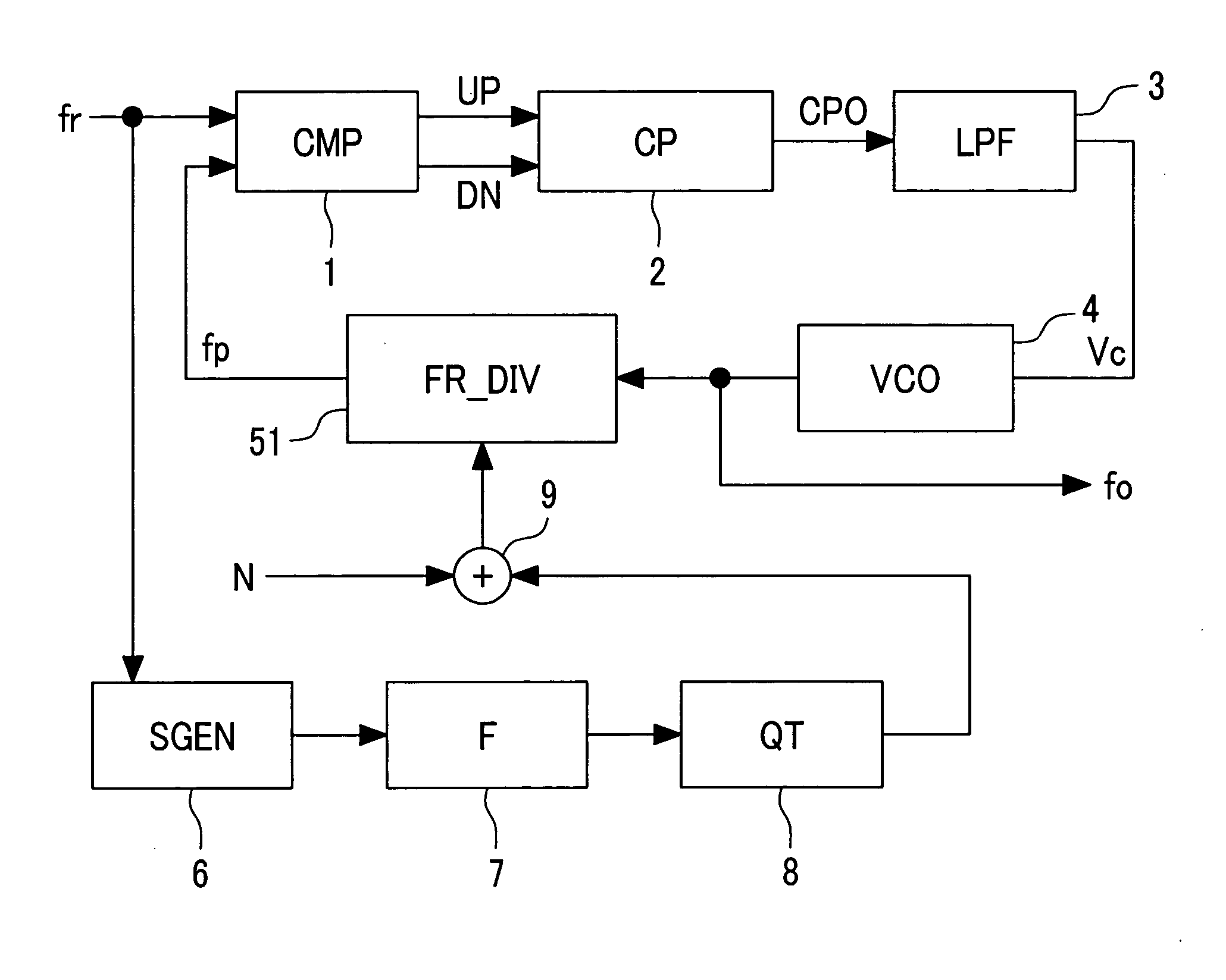
A first preferred embodiment of the present invention is discussed, using FIGS. 1 through 10. FIG. 1 is a basic structural diagram of a spread spectrum clock generator according to the present invention. The spread spectrum clock generator is made up of a phase comparator 1, a charge pump 2, a loop filter 3, a VCO 4, a fractional divider (FR_DIV) 51, a signal generator 6, a filter 7, a quantizer 8, and an adder 9. In this configuration, the quantizer 8 output and an average division number N are added and a signal having a value obtained by the addition is used to control a division number of the fractional divider 51.

The phase comparator 1 detects a phase difference between the reference clock fr and the output fp of the fractional divider 51 and outputs a control signal UP or DN. Here, the control signal UP increases the oscillation frequency of the following VCO 4 and the DN signal decreases the oscillation frequency. The two control signals (UP, DN) that ar...

embodiment 2

<Embodiment 2>

Next, a second preferred embodiment of the present invention is discussed. FIG. 11 is a structural diagram of a device in which the spread spectrum clock generator according to the present invention described in the Embodiment 1 section, using FIGS. 1 through 10 is applied as a clock generator of a microprocessor.

The device of Embodiment 2 consists of a reference clock generator (REF_CLKGEN) 21, the microprocessor 27, and peripheral ICs (PHE_ICs) 16-1 and 26-2. The microprocessor 27 is made up of the spread spectrum clock generator (SSCLK_GEN) 22 according to the present invention, a CPU 23, logic circuitry (LGGIC_CKT) 24, and I / O 25 for interfacing with the peripheral ICs 26-1 and 26-2.

The reference clock generator 21 may be a crystal oscillator or similar oscillator which generates a stable signal that can serve as a reference clock. The output of the reference clock generator 21 is input to the spread spectrum clock generator 22 which generates a spread sp...

embodiment 3

<Embodiment 3>

Next, a third preferred embodiment of the present invention is discussed. FIG. 12 is a structural diagram of a device like a personal computer (PC) comprising an CPU and individual integrated circuits connected to it, wherein the spread spectrum clock generator according to the present invention described in the Embodiment 1 section is applied. The personal computer essentially consists of the CPU 23, a memory bridge (MMBRG) 36 which performs data transfer to / from a memory (MM) 32 and a graphic memory (GMM) 33, and an I / O bridge integrated circuit 39 which includes an I / O bridge (I / O_BRG) 34 which makes connection to peripheral devices (PHEDs) 35-1, 35-2.

Here, in most cases, as the peripheral devices 35-1, 35-2, storage devices such as hard disks, DVDs (Digital Versatile Discs), and CDs (Compact Discs) are used. However, the personal computer configuration is not limited to that shown in FIG. 12 and the peripheral device types may vary, according to the purpose...


PUM


Abstract

The present invention provides a spread spectrum clock generator that is capable of preventing phase jumps and jitters and suppressing the occurrence of Electro Magnetic Interference components and that can easily be applied to large scale integrated circuits. The spread spectrum clock generator can be configured with a filter, quantizer, fractional divider, and other elements. Also, this clock generator circuitry can be configured by combination of a delta-sigma ΔΣ quantizer and factional divider so that sine wave modulation and random number modulation can be realized. Thereby, control with digital values can be performed. This clock generator prevents precipitous phase variations in the output high frequency clock and makes fine phase control possible. Consequently, EMI reduction by 20-30 dB can be expected.

Description

CLAIM OF PRIORITY The present application claims priority from Japanese patent application serial no. JP 2004-126341 filed on Apr. 22, 2004, which further claims priority from Japanese patent application serial no. JP 2003-194058 filed on Jul. 9, 2003, the contents of which are hereby incorporated by reference into this application. BACKGROUND OF THE INVENTION 1. Field of the Invention The present invention relates to circuitry which generates a clock for controlling signal processing devices integrated on a semiconductor chip. More particularly, the invention relates to a spread spectrum clock generator using a spread spectrum technique and an integrated circuit device employing the spread spectrum clock generator. 2. Description of the Related Art Signal processing devices integrated on a semiconductor chip, such integration being called a microprocessor, are often used for purposes such as generating a control signal for an appropriate control task from an input signal. In t...

Claims


Application Information

Patent Timeline
Patent Type & Authority Applications(United States)
IPC IPC(8): G06F1/04H03L7/08H03L7/183H03L7/197H04B15/04
CPCG06F1/03G06F1/04H04B2215/067H03L2207/06H04B15/04H03L7/197
Inventor KOKUBO, MASARUSHIBAHARA, YOSHIYUKI
Owner RENESAS ELECTRONICS CORP
Why Eureka
Try Eureka