Microstructures and methods of fabricating

a microstructure and fabrication method technology, applied in the field of microstructures, can solve the problems of low level of control over the placement of defects, poor suited to fabricating the complex designs required of optical circuitry, and limited to simple designs

Inactive Publication Date: 2005-01-20
MACQUARIE UNIV
View PDF11 Cites 35 Cited by
  • Summary
  • Abstract
  • Description
  • Claims
  • Application Information

AI Technical Summary

Problems solved by technology

Current methods for fabricating photonic crystals, such as colloidal sphere packing and 3-D laser intcrferometry, are suitable for producing generic photonic crystals with simple symmetrical designs but are poorly suited to fabricating the complex designs required of optical circuitry.
This technique offers a low level of control over the placement of defects and is generally limited to simple designs.
This is a disadvantage shared by another commonly used technique, namely 3 and 4 beam laser interferometry.
Conventional direct-write laser micro-machining provides for greater versatility in the design of the product, but has the disadvantage that it is limited by the laser spot size (at best 1 micron in diameter) to fabricating novel structures of 1 micron in size.
Full control over the placement of defects in otherwise regular arrays may be attained by using conventional femtosecond laser micro-machining, however, this is slow and hence poorly suited to mass production.
Furthermore, the definition of the unit cells in these periodic structures is generally poor.
Another disadvantage associated with current photonic crystal structures is the difficulty in coupling light into and out of these devices.

Method used


Image

  • Microstructures and methods of fabricating
  • Microstructures and methods of fabricating
  • Microstructures and methods of fabricating

Examples


example 1

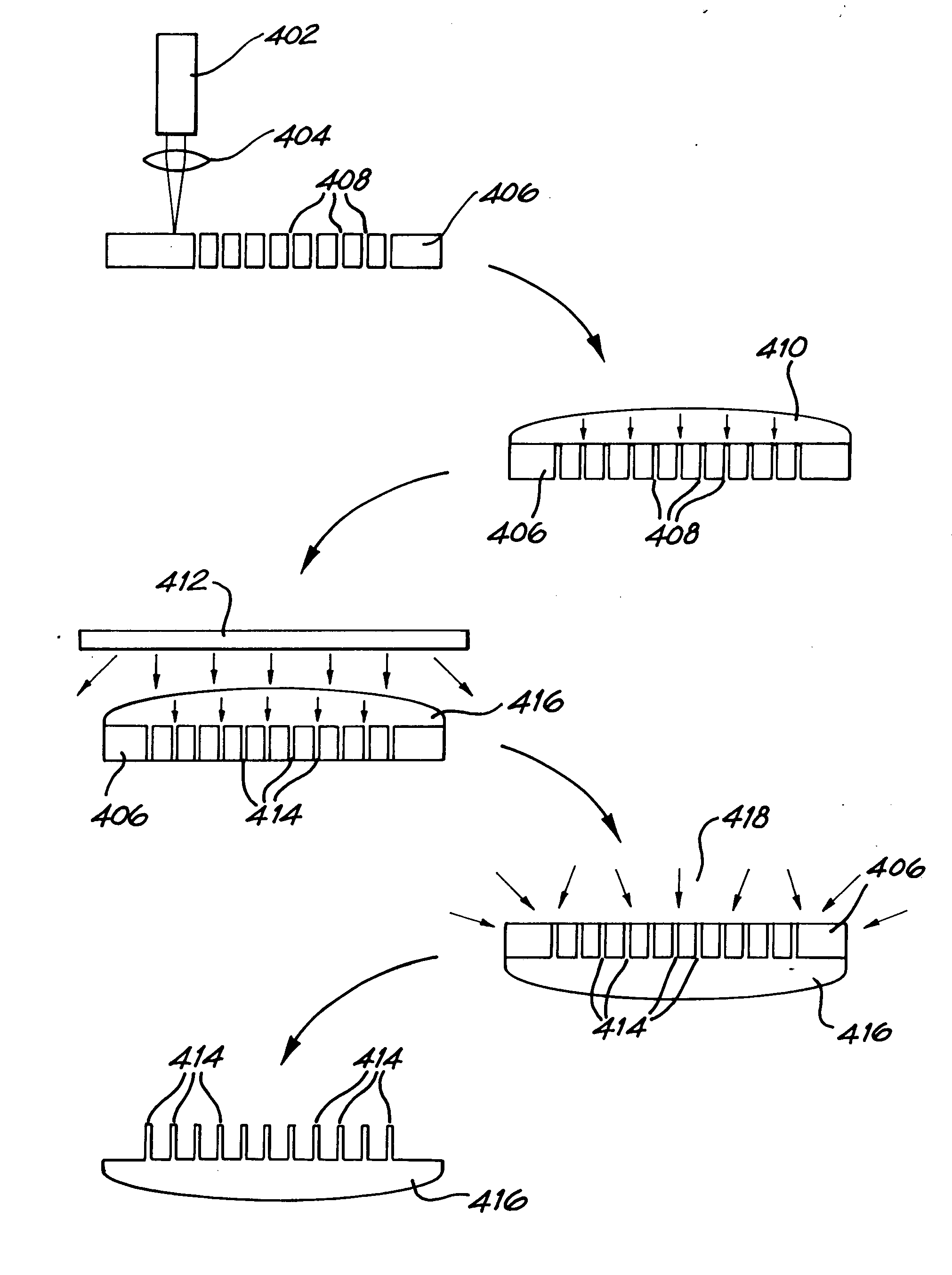
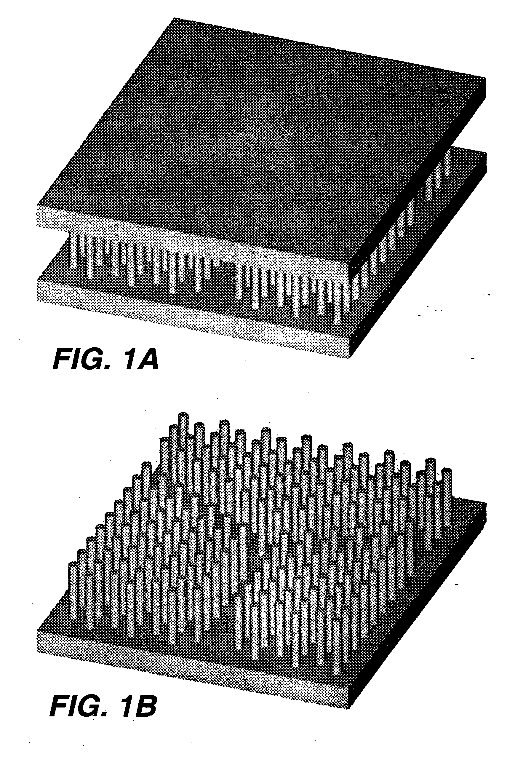
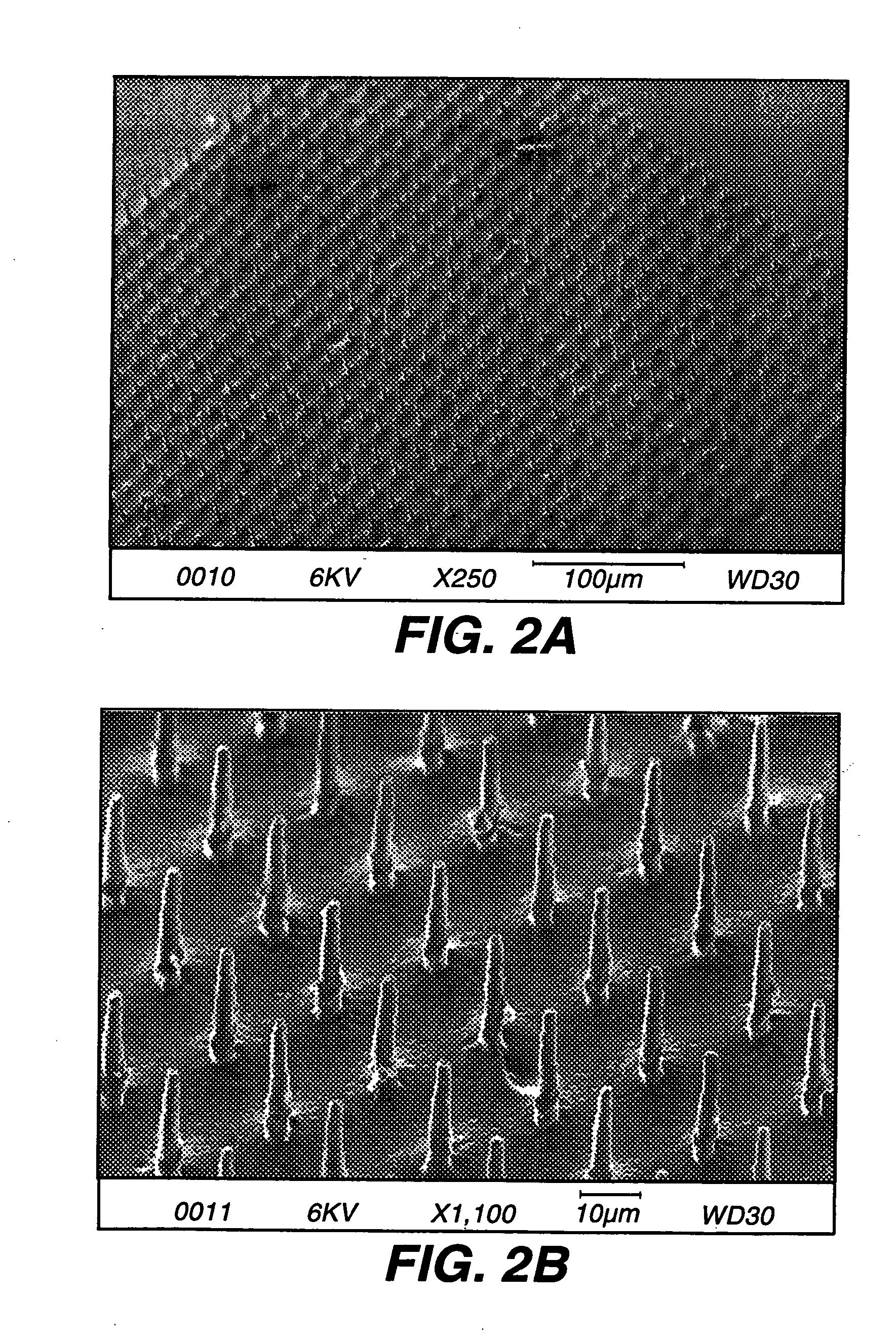
A photonic crystal was fabricated as follows. A template was formed in a polyolefin film by combining a laser based ablation process (using a UV, frequency-doubled copper-vapour laser, operating a wavelength of 255 nm) with a computer controlled stage and shutter arrangement. A triangular array which exhibits a band-gap was programmed into the computer. Using an average power of 30 mW and 100 ms exposure time, arrays of holes were formed in the polyolefin film. This constituted the template, which contained approximately 2 μm diameter holes. The template was then sandwiched between two microscope slides, which were spaced using cellulose tape, and the assembly placed on a hotplate at a temperature of 90° C. As a result the template shrunk, with the hole diameter reducing by a factor of five, while the spacing reduced by a factor of two.

The next step involved the filling of the template with a high refractive index material. Germanium was deposited onto the template. After deposit...

example 2

Method

In this experiment a frequency-doubled copper-vapour laser was used to process a range of different materials in a direct write manner. Frequency doubling was achieved using a beta-barium borate crystal, converting the 510 nm output to 255 nm. The laser was operated at a pulse rate of 10 kHz with a 40 ns pulse duration. Laser ablation using the ultra-violet, frequency-doubled output of these is well known and the characteristics of this laser made it ideal for material processing.

Various polymers including polycarbonate (PC), polyvinylchloride (PVC), polymethylmethacrylate (EMMA), polyolefin and polyethyleneterephthalateglycolate (PETG) were laser-processed. Each has significant absorption in the UV wavelength range, allowing photoablative processes to take place. Due to the copolymer matrix structure of polyolefin it exhibits a high degree of heat-shrinkability, and this property was used to further miniaturise the templates.

The templates were processed using computer ...

example 3

Novel Methods for Fabricating Photonic Crystal Like Structures

One of the most exciting materials to emerge in recent times is the photonic crystal. Various methods for fabricating photonic crystals have been reported. These include bottom-up micro-fabrication methods such as two-photon polymerisation of resins, opal templating, colloidal packing, self-assembly and stacking-micromanipulation processes, and top-down methods such as e-beam lithography, focussed ion beam etching and holography. These methods are capable of forming both two-dimensional (planar) and three-dimensional structures with varying degrees of complexity. However, the methods falling in the first group lack the degree of flexibility required to fabricate complex photonic crystal structures while those in the second have large infrastructure costs.

The recent demonstrations of sub-micron laser machining using ultrafast laser sources opens the way to top-down fabrication of photonic crystals using direct write l...


PUM

PropertyMeasurementUnit
refractive indicesaaaaaaaaaa
diameteraaaaaaaaaa
diameteraaaaaaaaaa

Abstract

A process of making a microstructure, is described. The process comprises the steps of forming a plurality of fillable features in a first material, to form a template; and applying a second material to the template so that the second material at least partially fills at least some of the fillable features in the template so as to form the microstructure, said second material being different from the first material. The process of forming a template uses a laser selected from a picosecond laser, a femtosecond laser and a nanosecond UV laser. The invention includes a photonic crytal made by this process.

Description

TECHNICAL FIELD The invention relates to microstructures such as photonic crystals and to processes for making them. BACKGROUND ART There is considerable interest in fabricating periodic sub-micron structures in optical materials, termed photonic crystals, and other microstructures for use in the telecommunication industry. These devices will form the optical equivalent of conventional electronic circuitry with the ultimate aim being the realisation of all-optical computer chips. Photonic crystal microstructures are the precursors to all-optical computer chips and are viewed as forming the basis of next generation telecommunications and computing systems. Current methods for fabricating photonic crystals, such as colloidal sphere packing and 3-D laser intcrferometry, are suitable for producing generic photonic crystals with simple symmetrical designs but are poorly suited to fabricating the complex designs required of optical circuitry. There are a number of patents covering 3-D,...

Claims


Application Information

Patent Timeline
Patent Type & Authority Applications(United States)
IPC IPC(8): B23K26/06B23K26/40G02B6/122G02B6/13
CPCB23K26/0656B23K26/365B23K26/4065B23K26/4075B23K26/0635B82Y20/00G02B6/1225G02B6/13B23K26/0084B23K2201/40B23K26/0624B23K26/066B23K26/40B23K26/361B23K26/355B23K2101/40B23K2103/42B23K2103/50
Inventor WITHFORD, MICHAEL J.BAER, DAVIDLEE, ANDREWDAWES, JUDITH M.
Owner MACQUARIE UNIV
Why Eureka
Try Eureka