Semiconductor device manufacturing method
a manufacturing method and semiconductor technology, applied in the direction of semiconductor/solid-state device details, liquid/solution decomposition chemical coating, coating, etc., can solve the problems of weak electro-migration resistance at the interface between sin or sic constituting the barrier film and copper, high effective dielectric constant of the semiconductor device including the copper wiring, and high rc delay (delay of the wiring). , to achieve the effect of high efficiency, high quality and simplified manufacturing steps
- Summary
- Abstract
- Description
- Claims
- Application Information
AI Technical Summary
Benefits of technology
Problems solved by technology
Method used
Image

Examples
Embodiment Construction
[0045] Now, the method of manufacturing a semiconductor device according to the present invention will be described in detail below referring to the drawings. The present invention is not limited to the following description, and various modifications are possible within the gist of the invention. First, the case where the present invention is applied to a monolayer wiring will be described. In the following drawings, the contraction scale may differ from the actual one, for convenience of description.
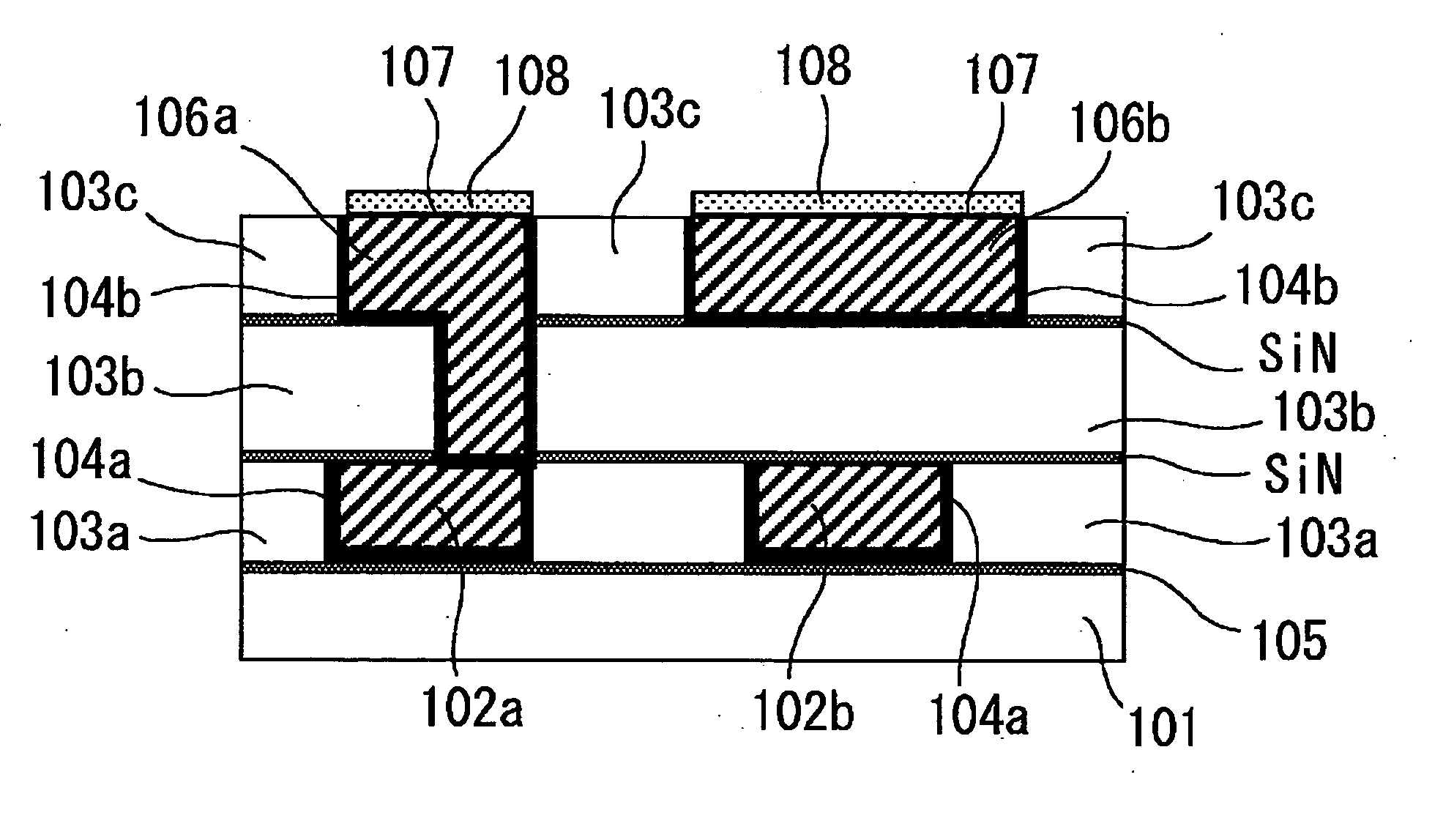
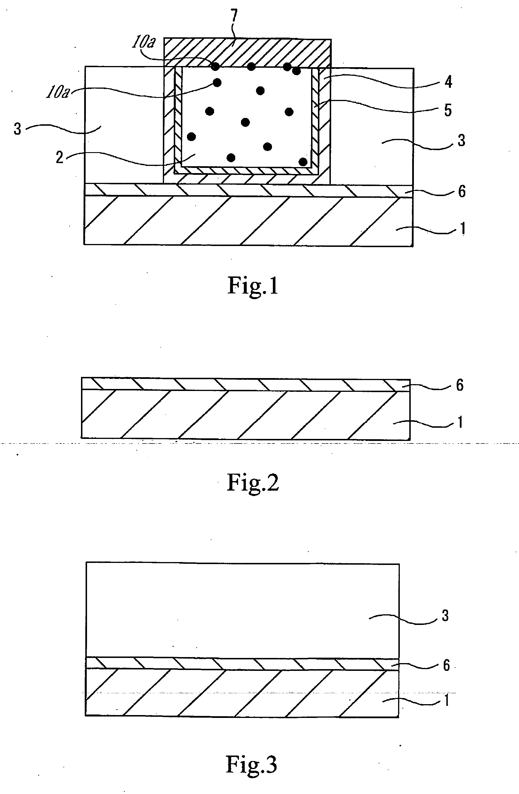
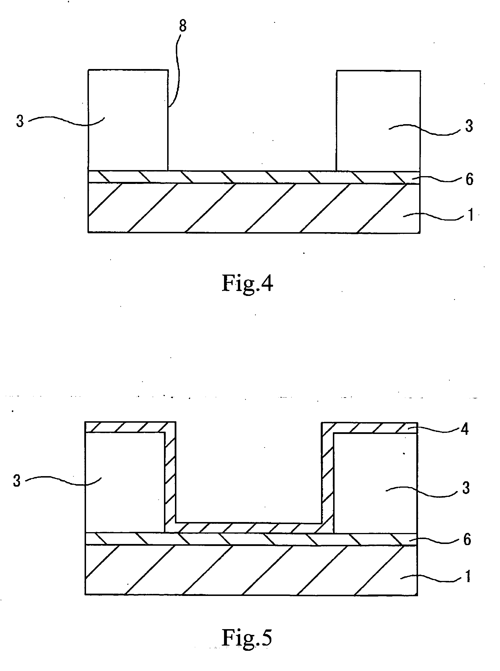
[0046]FIG. 1 is a sectional view of an essential part of a semiconductor device produced by applying the present invention. The semiconductor device includes a copper-containing metallic wire, on which is formed a barrier film having a copper diffusion preventive function. The semiconductor device has a configuration in which the copper-containing metallic wire (hereinafter referred to as Cu wiring) 2 is filling a groove provided in an inter-layer insulating film 3, on a substrate 1 p...
PUM
| Property | Measurement | Unit |
|---|---|---|
| Temperature | aaaaa | aaaaa |
| Temperature | aaaaa | aaaaa |
| Temperature | aaaaa | aaaaa |
Abstract
Description
Claims
Application Information
 - R&D
- Intellectual Property
- Life Sciences
- Materials
- Tech Scout
- Unparalleled Data Quality
- Higher Quality Content
- 60% Fewer Hallucinations
Browse by: Latest US Patents, China's latest patents, Technical Efficacy Thesaurus, Application Domain, Technology Topic, Popular Technical Reports.
© 2025 PatSnap. All rights reserved.Legal|Privacy policy|Modern Slavery Act Transparency Statement|Sitemap|About US| Contact US: help@patsnap.com