Semiconductor device method of generating semiconductor device pattern method of semiconductor device and pattern generator for semiconductor device

a semiconductor device and semiconductor technology, applied in the field of semiconductor devices, can solve the problems of increasing the number of components, radio interference of the receiver, and malfunction of other systems, and achieve the effect of reducing power noise and increasing capacity

Active Publication Date: 2005-01-27
PANASONIC SEMICON SOLUTIONS CO LTD
View PDF1 Cites 10 Cited by
  • Summary
  • Abstract
  • Description
  • Claims
  • Application Information

AI Technical Summary

Benefits of technology

[0019] It is yet another object of the invention to form a capacitor having a larger cap

Problems solved by technology

On the other hand, however, there are problems in that an electromagnetic interference (EMI) generated from these products causes the radio interference of a receiver such as a television or a radio and the malfunction of other systems.
In respect of an increase in the number of components, an increase in a cost and the difficulty of a countermeasure in a product, the noise suppression of an LSI package has been greatly demanded.
Consequently, an increase in the electromagnetic interference is caused.
With the microfabrication of the LSI and an increase in the speed of an operating frequency, thus, countermeasures against latch up and a noise have been great proble

Method used


Image

  • Semiconductor device method of generating semiconductor device pattern method of semiconductor device and pattern generator for semiconductor device
  • Semiconductor device method of generating semiconductor device pattern method of semiconductor device and pattern generator for semiconductor device
  • Semiconductor device method of generating semiconductor device pattern method of semiconductor device and pattern generator for semiconductor device

Examples


first embodiment

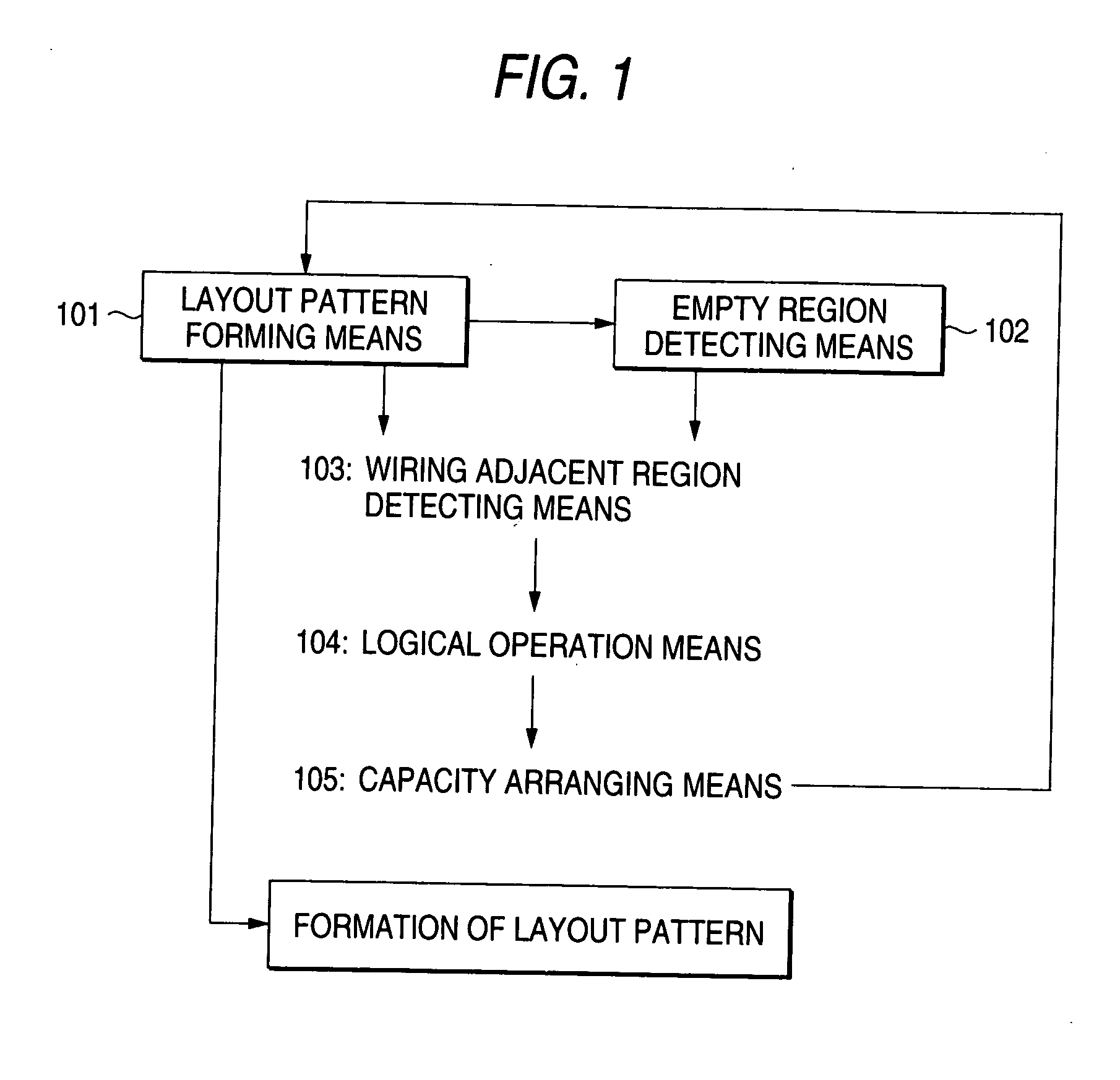
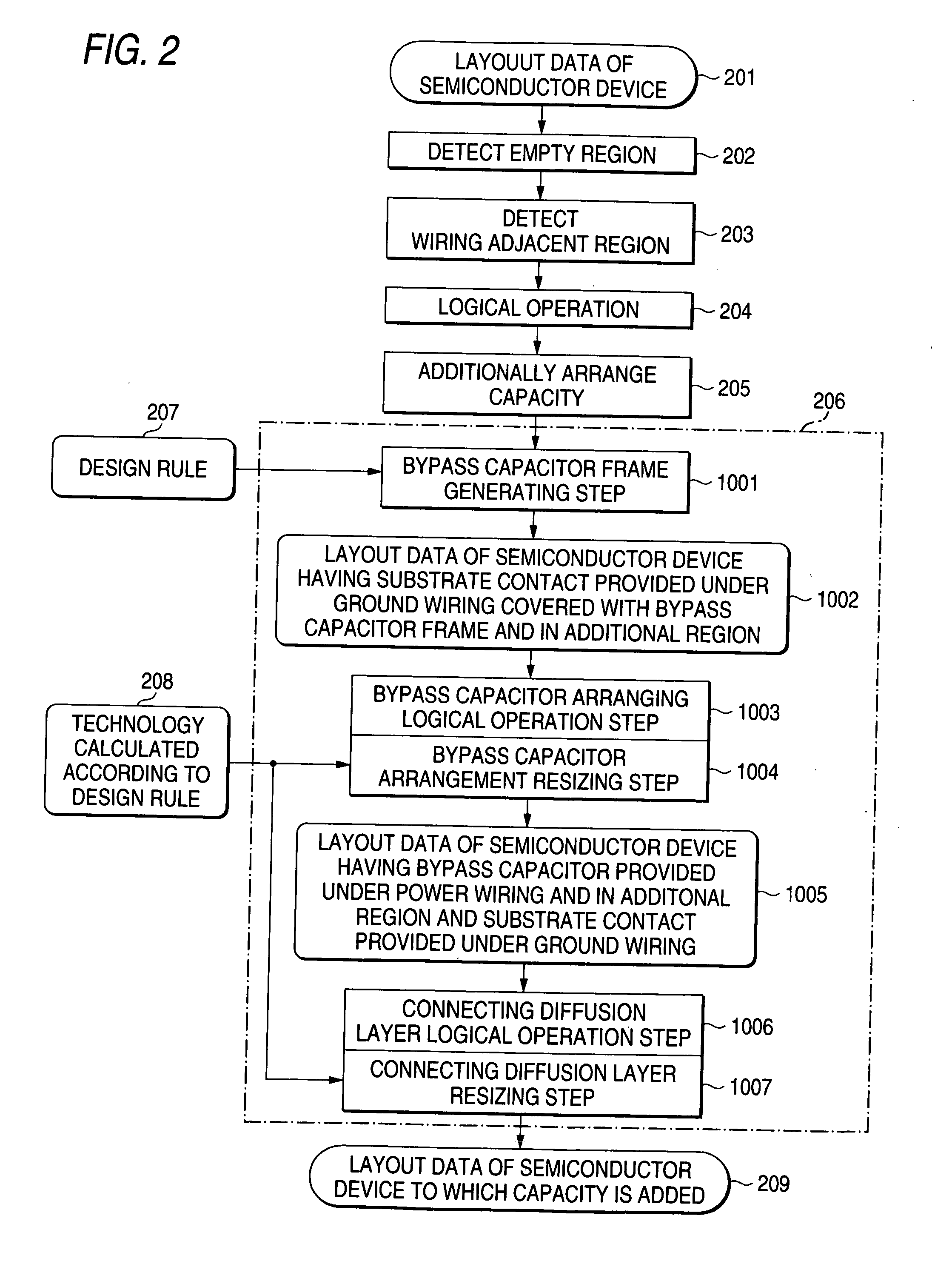
[0110]FIG. 1 is a block diagram showing a pattern generating apparatus according to an embodiment of the invention. The apparatus comprises layout pattern forming means 101 for designing and arranging the layout pattern of a semiconductor chip, empty region detecting means 102 for detecting an empty region in which the layout pattern is not present on the semiconductor chip, wiring adjacent region detecting means 103 for detecting an adjacent region to a wiring region from the layout pattern formed by the layout pattern forming means, logical operation means 104 for carrying out a logical operation over a region detected by the empty region detecting means and a wiring region detected by the wiring adjacent region detecting means, and capacity arranging means 105 for setting a region extracted by the logical operation means to be a decoupling capacity additional arrangement region, and has such a structure that a decoupling capacity is additionally provided in the empty region and l...

second embodiment

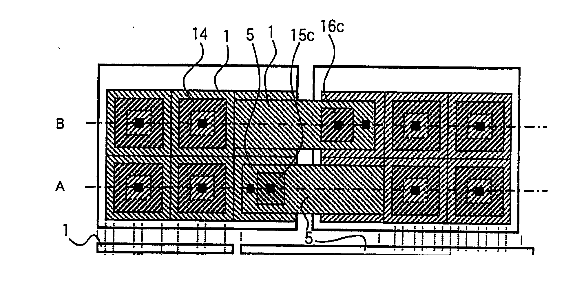
[0133] While the description has been given to the example in which the bypass capacitor having the MOS structure using the diffusion region having a reverse conductivity type to that of the substrate (P well) is formed under the power wiring region extended to the empty region and is connected through a salicide process, a bypass capacitor having an MOS structure using a diffusion region having the same conductivity type as that of a substrate (P well) is automatically arranged as a bypass capacitor and a substrate contact provided under a ground wiring and the bypass capacitor provided under a power wiring are connected to each other through a diffusion in this example.

[0134] More specifically, FIGS. 7(a) to 7(c) are plan views (FIGS. 7(b) and 7(c) are A-A and B-B sectional views of FIG. 7(a) respectively) in which a bypass capacitor having an MOS structure using a substrate contact under a ground wiring and a diffusion region having the same conductivity type as that of a substr...

third embodiment

[0137] While the description has been given to the example in which the bypass capacitor having the MOS structure using the diffusion region having a reverse conductivity type to that of the substrate (P well) is formed under the power wiring region extended to the empty region and is connected through the salicide process in the first embodiment, an N+ type diffusion region 15e (a diffusion region having a different conductivity type from that of a substrate (P well)) extended for bypass capacitor formation is further extended to a part of a substrate contact formation region and both a substrate contact 7 provided in contact with a contact diffusion region 16 under a ground wiring 5 and a connecting contact 7s provided in contact with the extended N+ type diffusion region 15e are connected to the ground wiring 5 in a substrate contact region as shown in FIGS. 8(a) to 8(c) (FIGS. 8(b) and 8(c) are A-A and B-B sectional views of FIG. 8(a) respectively) in this example.

[0138] Other ...


PUM


Abstract

It is an object of the invention to effectively absorb a power noise and to implement the stable operation of a circuit. The invention provides a semiconductor device comprising a bypass capacitor including an MOS structure having a gate electrode formed to be extended from a power wiring region to a portion provided under an empty region which is adjacent to the power wiring region and has no other functional layer, and formed through a capacitive insulating film on a diffusion region having one conductivity type, and a substrate contact formed under a ground wiring region and fixing a substrate potential, wherein the bypass capacitor has a contact to come in contact with the power wiring which is formed on a surface of the gate electrode and has the diffusion region having the one conductivity type and a diffusion region of the substrate contact connected to each other.

Description

TECHNICAL FIELD [0001] The present invention relates to a semiconductor device, a method of generating a semiconductor device, a method of manufacturing a semiconductor device and an apparatus for generating a semiconductor device, and more particularly to a semiconductor device including a bypass capacitor and an inductor for a countermeasure against a noise of the semiconductor device, and a method of generating a pattern thereof. BACKGROUND ART [0002] As a matter of course, the utilization scope of an LSI in a computer has been enlarged for communicating apparatuses such as a portable telephone, general household appliances, toys and cars. On the other hand, however, there are problems in that an electromagnetic interference (EMI) generated from these products causes the radio interference of a receiver such as a television or a radio and the malfunction of other systems. A countermeasure in the whole products such as filtering or shielding has also been taken against these probl...

Claims


Application Information

Patent Timeline
IPC IPC(8): G06F17/50H01L21/82H01L21/822H01L27/02H01L27/04
CPCH01L27/0207G06F17/5068G06F30/39
Inventor ITOH, MITSUMISAWADA, MASATOSHIHONMA, JUNKOSHIMAZAKI, KENJITSUJIKAWA, HIROYUKIBENNO, HIROSHI
Owner PANASONIC SEMICON SOLUTIONS CO LTD
Why Eureka
Try Eureka