

Semiconductor memory device
a memory device and semiconductor technology, applied in semiconductor devices, digital storage, instruments, etc., can solve the problems of increasing chip cost, large chip size, and increasing manufacturing steps, and achieve large memory capacity and small occupancy area. , the effect of not increasing the number of manufacturing steps significantly
- Summary
- Abstract
- Description
- Claims
- Application Information
AI Technical Summary
Benefits of technology
Problems solved by technology
Method used
Image

Examples
first embodiment
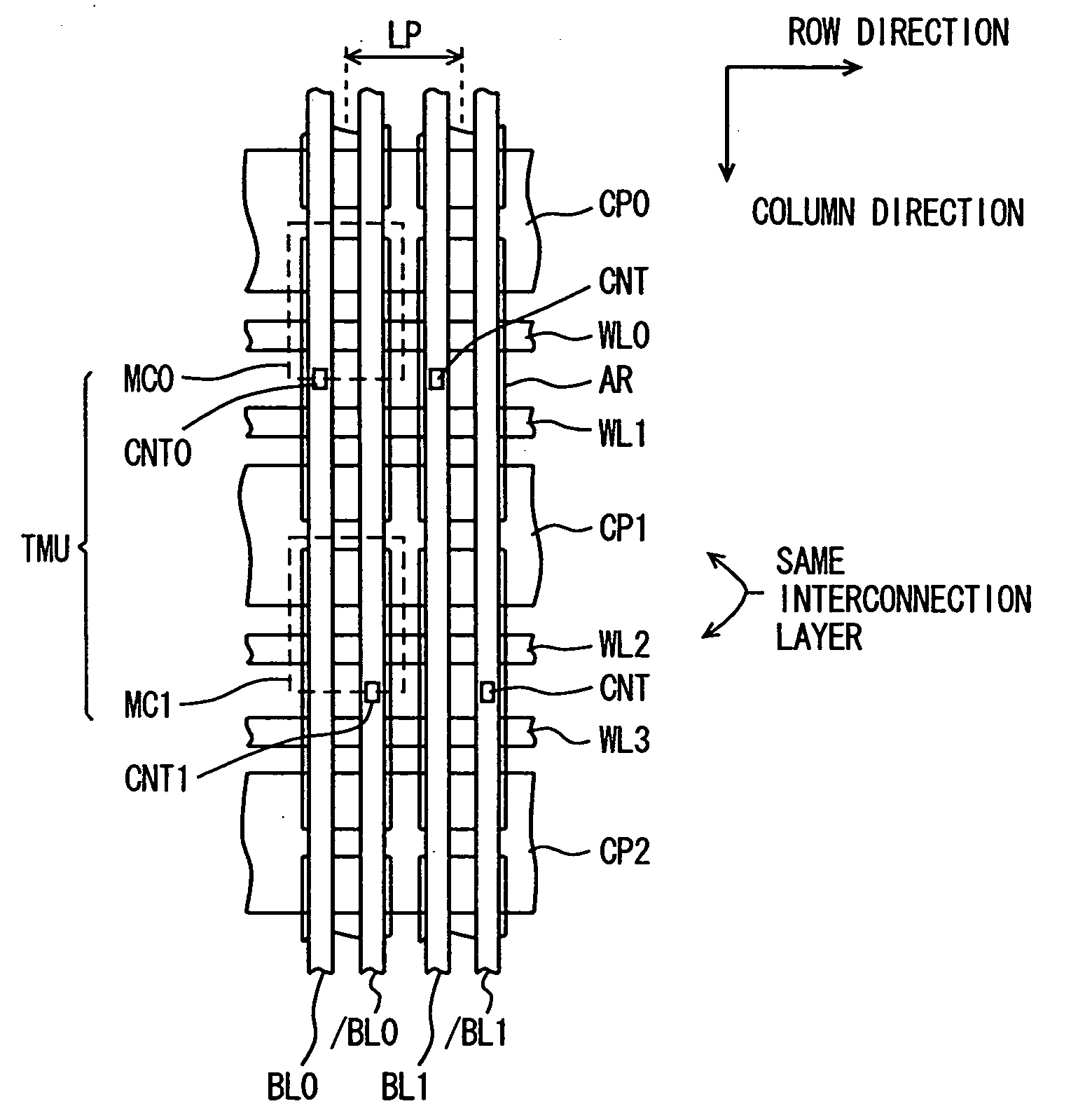
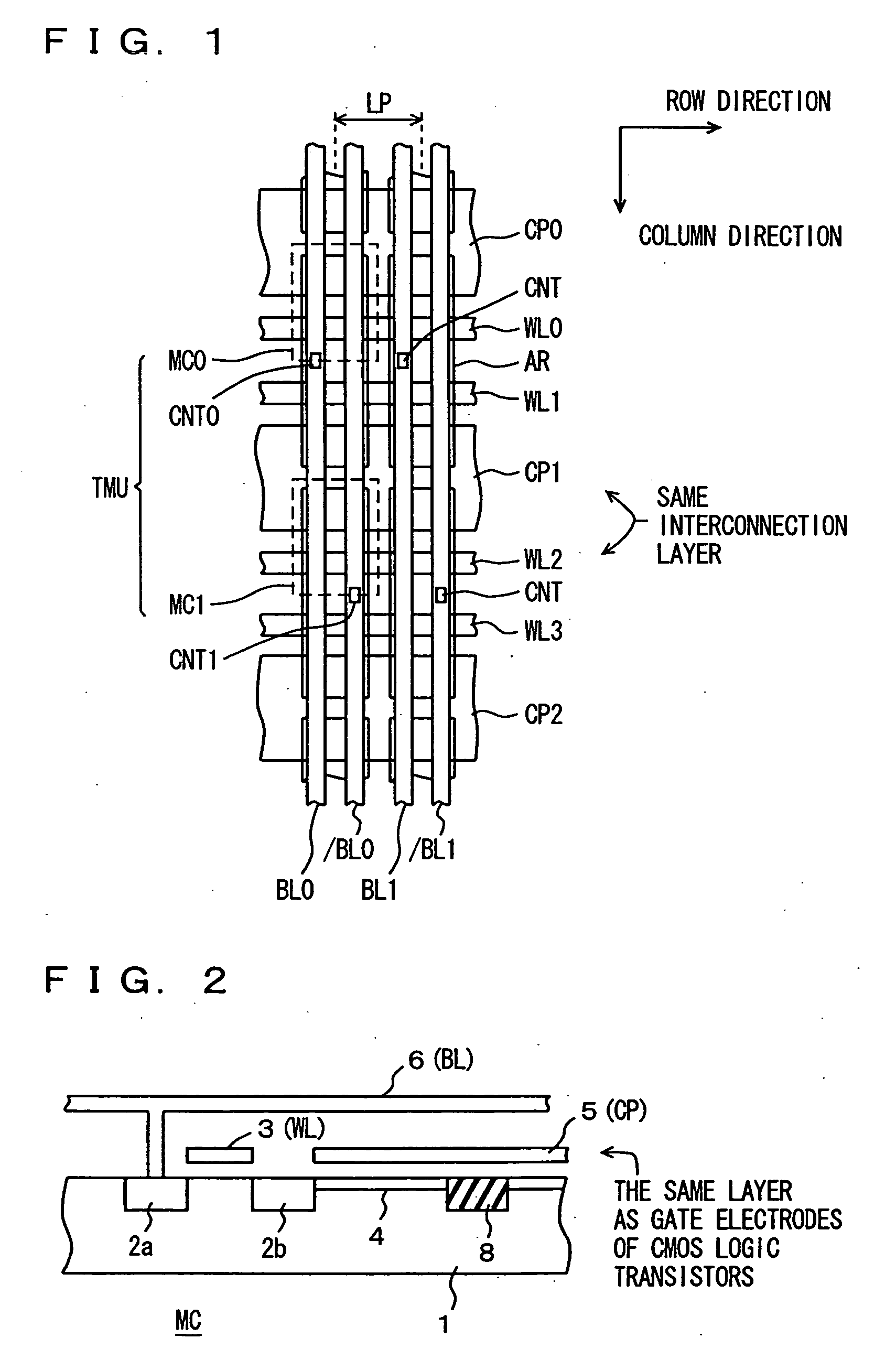
FIG. 1 is a diagram schematically showing the configuration of an array section of a semiconductor memory device according to a first embodiment of the present invention. A layout of memory cells arranged in 4 rows and 2 columns is shown representatively in FIG. 1. In FIG. 1, word lines WL0-WL3 are arranged extending in the row direction. Cell plate electrode lines CP0-CP2 are formed in the same interconnection layer as word lines WL0-WL3 and in parallel to these word lines. Accordingly, cell plate electrode lines CP0-CP2 are arranged such that adjacent cell plate lines sandwich two word lines, and are arranged extending in the row direction in the memory cell array. The cell plate electrode lines adjacent to each other in the column direction are separated from each other by a word line WL arranged in between.
Word line WL0-WL3 are arranged corresponding to memory cell rows, and are connected to the memory cells in corresponding rows.
second embodiment
FIG. 7 is a diagram schematically showing a layout of a memory array according to a second embodiment of the present invention. In the layout illustrated in FIG. 7, active areas AR for forming memory cells are arranged in a staggered arrangement in the column direction such that active areas AR are shifted by ½ of pitch Lp of the memory cells in the row direction. The other configurations are the same as in the layout illustrated in FIG. 1. Therefore, in the arrangement of the memory cells illustrated in FIG. 7, with the two memory cells adjacent in the column direction being one unit, and a plurality of the memory cell layout units are arranged in the column direction with the pitch of the one bit line deviated. Two bit lines BL (BL0- / BL1) are arranged in pitch LP in the row direction of the memory cells.
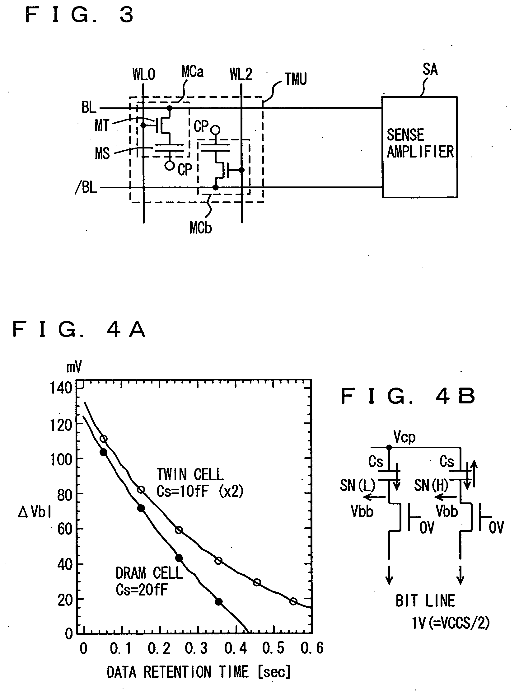
Upon selecting memory cells, two word lines, for example, word lines WL0 and WL2 are simultaneously selected. Storage data in a memory cell MC0 is read out onto bit line BL0 thro...
third embodiment
FIG. 9 is a diagram schematically showing a layout of a memory array according to a third embodiment of the present invention. The layout of memory cells illustrated in FIG. 9 is the same as the layout of the memory array illustrated in FIG. 7. In the configuration illustrated in FIG. 9, adjacent bit lines do not constitute a bit line pair. A bit line pair is provided by two bit lines with one bit line interposed in between. Upon selection of a word, one of word lines is selected. Therefore, memory cells MC0 and MC3 constitute a twin cell unit TMU, and memory cells MC1 and MC4 constitute another twin cell unit. The other configurations are the same as in FIG. 7. The same reference numerals are allotted to the corresponding components, and detailed explanation thereof is omitted.
In the configuration as illustrated in FIG. 9, one of the word lines is selected, but two word lines do not need to be selected. Thus, current consumption can be reduced.
A bit line onto which no memory ce...
PUM
 Abstract
Description
Claims
Application Information