Method of controlling a capacitance of a thin film transistor liquid crystal display (TFT-LCD) storage capacitor

a technology of liquid crystal display and storage capacitor, which is applied in the direction of instruments, semiconductor devices, optics, etc., can solve the problems of inability to design tft dimensions according, affecting the thickness uniformity of the storage capacitor dielectric layer in each pixel, and poor thickness uniformity of the gate dielectric layer after over-etching on the entire transparent substrate. achieve uniform thickness, improve display quality, and increase the aperture ratio of each pixel

Inactive Publication Date: 2005-02-10
HANNSTAR DISPLAY CORPORATION
View PDF11 Cites 0 Cited by
  • Summary
  • Abstract
  • Description
  • Claims
  • Application Information

AI Technical Summary

Benefits of technology

[0008] One aspect of the invention provides a method of controlling the capacitance of the TFT-LCD storage capacitor to control the uniformity of the storage capacitor's dielectric layer.
[0009] Another aspect of the invention provides a method of controlling the capacitance of the TFT-LCD storage capacitor to improve the uniformity of the storage capacitor's capacitance.
[0016] Various inventive embodiments allow the dielectric layer to be an etch stop layer when the stacked layer is formed, and the remaining dielectric layer and the first silicon nitride layer thus have a uniform thickness. Therefore, the storage capacitor, which comprises overlapping parts of the bottom electrode, the first silicon nitride layer, the dielectric layer, the passivation layer and the pixel electrode, has a uniform dielectric layer, which comprises the first silicon nitride layer, the dielectric layer, and the passivation layer. As a result, the capacitance of the storage capacitor is also uniform to allow a smaller dimension of the thin film transistor. Hence, the aperture ratio of each pixel is increased to improve the display quality.

Problems solved by technology

Since the area of the transparent substrate is very large, the thickness uniformity of the gate dielectric layer after over-etching on the entire transparent substrate is not good.
Thus, the thickness uniformity of the storage capacitor dielectric layer in each pixel is also affected.
Therefore, the TFT dimensions cannot be designed according to the ideal condition that each storage capacitor has the same capacitance.

Method used


Image

  • Method of controlling a capacitance of a thin film transistor liquid crystal display (TFT-LCD) storage capacitor
  • Method of controlling a capacitance of a thin film transistor liquid crystal display (TFT-LCD) storage capacitor
  • Method of controlling a capacitance of a thin film transistor liquid crystal display (TFT-LCD) storage capacitor

Examples


embodiment 1

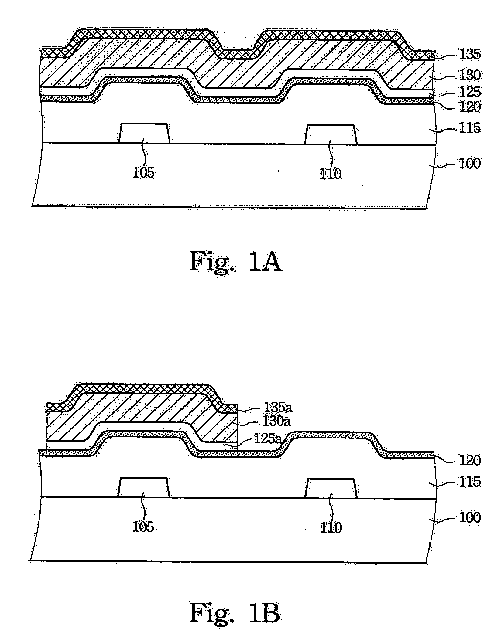
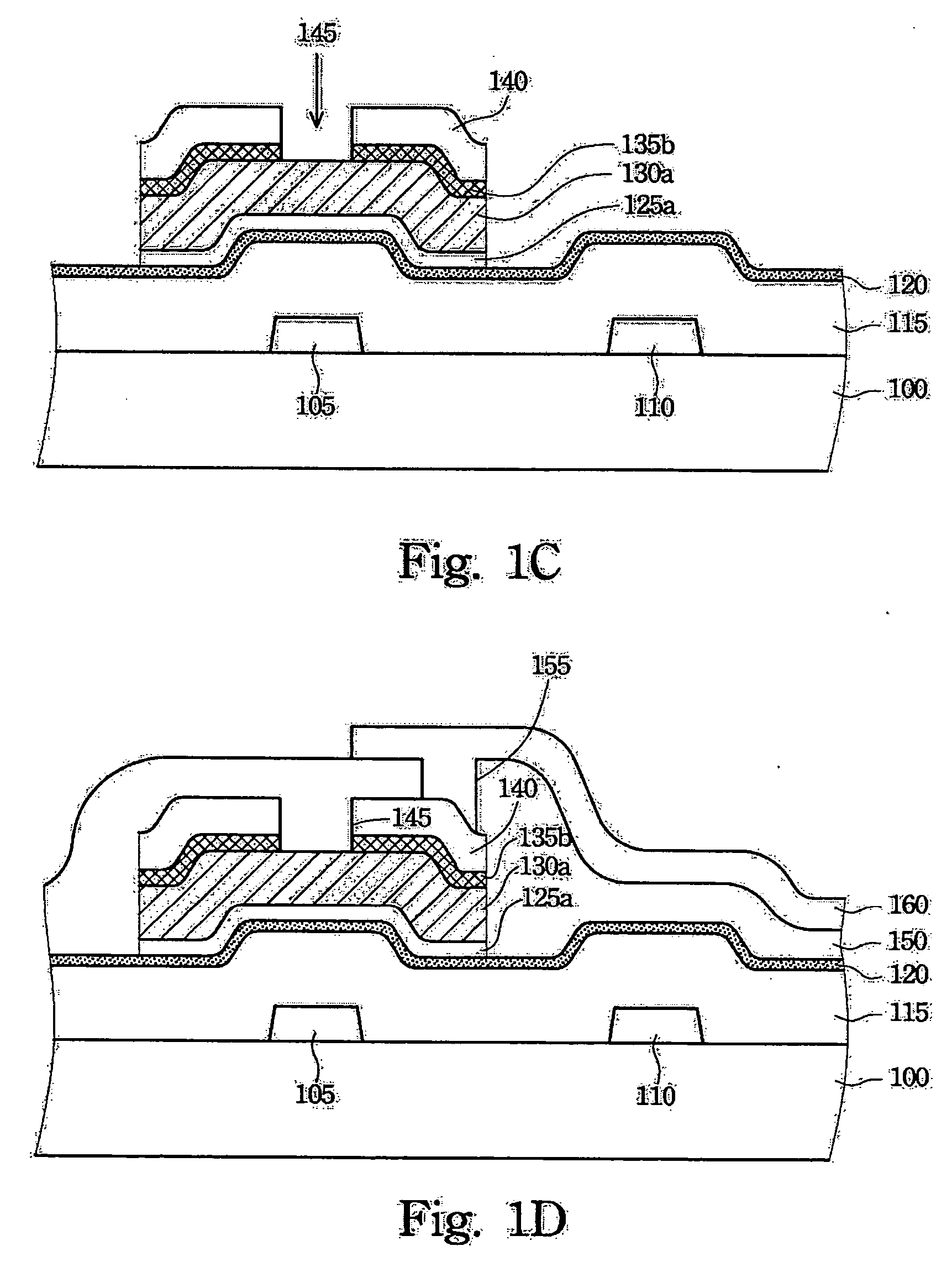
[0024]FIGS. 1A-1D are schematic, cross-sectional views showing a process for controlling the capacitance of the TFT-LCD storage capacitor according to a first preferred embodiment of this invention. In FIG. 1A, a first conductive layer is formed on a transparent substrate 100 and then is patterned to form a gate 105 and a bottom electrode 110 respectively on the transparent substrate 100. Then, a first silicon nitride layer 115, a dielectric layer 120, a second silicon nitride layer 125, an undoped amorphous silicon layer 130, and a doped amorphous silicon layer 135 are sequentially formed on the transparent substrate.

[0025] The material of the first conductive layer is, for example, copper, aluminum. chromium or alloy of molybdenum and tungsten, and the first conductive layer can be formed by a physical vapor deposition process such as sputtering. The first silicon nitride layer 115 and the second silicon nitride layer 125 can be formed by chemical vapor deposition; the preferable...

embodiment 2

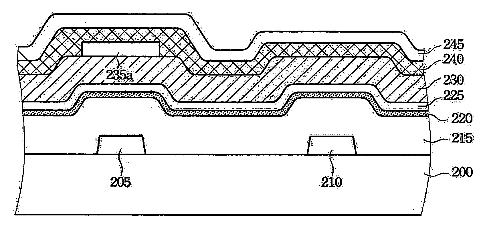
[0029]FIGS. 2A-2C are schematic, cross-sectional views showing a process for controlling the capacitance of the TFT-LCD storage capacitor according to a second preferred embodiment of this invention. In FIG. 2A, a first conductive layer is formed on a transparent substrate 200 and then is patterned to form a gate 205 and a bottom electrode 210 on the transparent substrate 200. A first silicon nitride layer 215, a dielectric layer 220, a second silicon nitride layer 225, an undoped amorphous silicon layer 230, and an etching stop layer 235 are sequentially formed on the transparent substrate 200.

[0030] The material of the first conductive layer is, for example, copper, aluminum, chromium or alloy of molybdenum and tungsten, and the first conductive layer is formed by a physical vapor deposition process such as sputtering. The first silicon nitride layer 215 and the second silicon nitride layer 225 is formed by chemical vapor deposition; the preferable thicknesses of the first silico...

embodiment 3

[0033]FIGS. 3A-3C are schematic, cross-sectional views showing a process of controlling the capacitance of the TFT-LCD storage capacitor according to a third preferred embodiment of this invention. In FIG. 3A, an undoped amorphous silicon layer is formed on a transparent substrate 300 and then is patterned to form a silicon island 305 and a bottom electrode 310 on the transparent substrate 300. A first silicon nitride layer 315, a dielectric layer 320, a second silicon nitride layer 325, and a first conductive layer 330 are sequentially formed on the transparent substrate 300.

[0034] The first silicon nitride layer 315 and the second silicon nitride layer 325 is formed by chemical vapor deposition; the preferable thicknesses of the first silicon nitride layer 315 and the second silicon nitride layer 325 are respectively about 1500-3500 Å and about 200-800 Å, and their more preferable thicknesses are respectively about 2000-3000 Å and about 400-600 Å. An etching selectivity ratio of ...


PUM

PropertyMeasurementUnit
dielectric constantaaaaaaaaaa
transparentaaaaaaaaaa
capacitanceaaaaaaaaaa

Abstract

A method of controlling the capacitance of a thin film transistor liquid crystal display (TFT-LCD) storage capacitor is disclosed. In certain embodiments, the method includes i) forming a silicon island and a bottom electrode on the transparent substrate, the silicon island having an undoped region located on the central portion, and two doped regions respectively located on both sides, ii) forming a first silicon nitride layer on the transparent substrate, and iii) forming a stacked layer comprising a second silicon nitride layer and a conductive layer on the undoped region of the silicon island, and the first conductive layer of the stacked layer serving as a gate of a thin film transistor, wherein an etching selectivity ratio of the conductive layer over the dielectric layer is not less than about 5.0.

Description

RELATED APPLICATIONS [0001] This application is a divisional application of U.S. application Ser. No. 10 / 289,470, filed Nov. 6, 2002, the full disclosure of which is incorporated herein by reference.BACKGROUND OF INVENTION [0002] 1. Field of Invention [0003] The present invention relates to a thin film transistor liquid crystal display (TFT-LCD). More particularly, the present invention relates to a method of controlling the capacitance of a TFT-LCD storage capacitor. [0004] 2. Description of the Related Art [0005] Liquid crystal display (LCD) has many advantages over other conventional types of displays including high display quality, small volume occupation, lightweight, low voltage driven and low power consumption. Hence, LCDs are widely used in small portable televisions, mobile telephones, video recording units, notebook computers, desktop monitors, projector televisions and so on. Therefore, LCD has gradually replaced the conventional cathode ray tube (CRT) as a mainstream dis...

Claims


Application Information

Patent Timeline
Patent Type & Authority Applications(United States)
IPC IPC(8): G02F1/1362H01L21/77H01L21/84H01L27/12H01L27/13H01L29/423
CPCG02F1/136213H01L27/1248H01L27/1255H01L29/42384
Inventor PENG, CHIH-YULIN, WEI-CHUANHSIAO, CHIAN-CHIHCHUANG, TA-KOCHU, CHUN-HUNGLIN, CHIH-LUNGLIN, CHIN-MAO
Owner HANNSTAR DISPLAY CORPORATION
Why Eureka
Try Eureka