
High performance embedded semiconductor memory devices with multiple dimension first-level bit-lines

a semiconductor memory and embedded technology, applied in semiconductor devices, digital storage, instruments, etc., can solve the problems of low performance, low density, and low performance of current art drams, and achieve the effects of improving the performance of semiconductor memory devices, improving user experience, and simplifying system suppor

Inactive Publication Date: 2005-02-17
UNIRAM TECH
View PDF74 Cites 27 Cited by
  • Summary
  • Abstract
  • Description
  • Claims
  • Application Information

AI Technical Summary

Benefits of technology

The primary objective of this invention is, therefore, to improve the performance of semiconductor memory device without paying extensive area penalty. Another primary objective is to make DRAM more user-friendly by making the performance improvement in parallel with simplification in system supports. Another primary objective is to provide an improved semiconductor memory device in which peripheral circuits can readily follow further higher integration of memory cells. Another objective is to reduce power consumption of high performance semiconductor memory.
(8) The simplification in manufacturing process results in significant improvements in product reliability and cost efficiency.

Problems solved by technology

DRAM is usually considered as a high density, low cost, but low performance memory device.
DRAM's of current art always have lower performance relative to other types of semiconductor memories such as static random access memory (SRAM).
This relatively slower improvement rate in performance generates a performance gap between logic devices and memory devices.
The major problem for above approaches is that they are paying very high price for performance improvement, while the resulting memory performance improvement is still not enough to fill the gap.
Another problem is that all of those approaches require special system design that is not compatible with existing computer systems; it is therefore more difficult to use them in existing computer systems.
Another disadvantage of DRAM is the need to refresh its memory.
The system support for DRAM is more complex than SRAM because of this memory refresh requirement.
Memory refresh also represents a waste in power.
The resource conflict problem between refresh and normal memory operations also remains unsolved by those patents.
The new device is not compatible with existing memory; it requires special system supports to handle conflicts between memory read operation and memories refresh operation.
It requires 30% more area the DRAM, and its performance is still worse than SRAM of the same size.
Another important problem for DRAM design is the tight pitch layout problem of its peripheral circuits.
When the memory cells are smaller for every new generation of technology, it is more and more difficult to “squeeze” peripheral circuits into small pitch of memory layout.
Although the available layout pitch is wider than conventional DRAM, the layout pitch is still very small using Yamauchi's approach.
All of the above inventions and developments provided partial solutions to memory design problems, but they also introduced new problems.
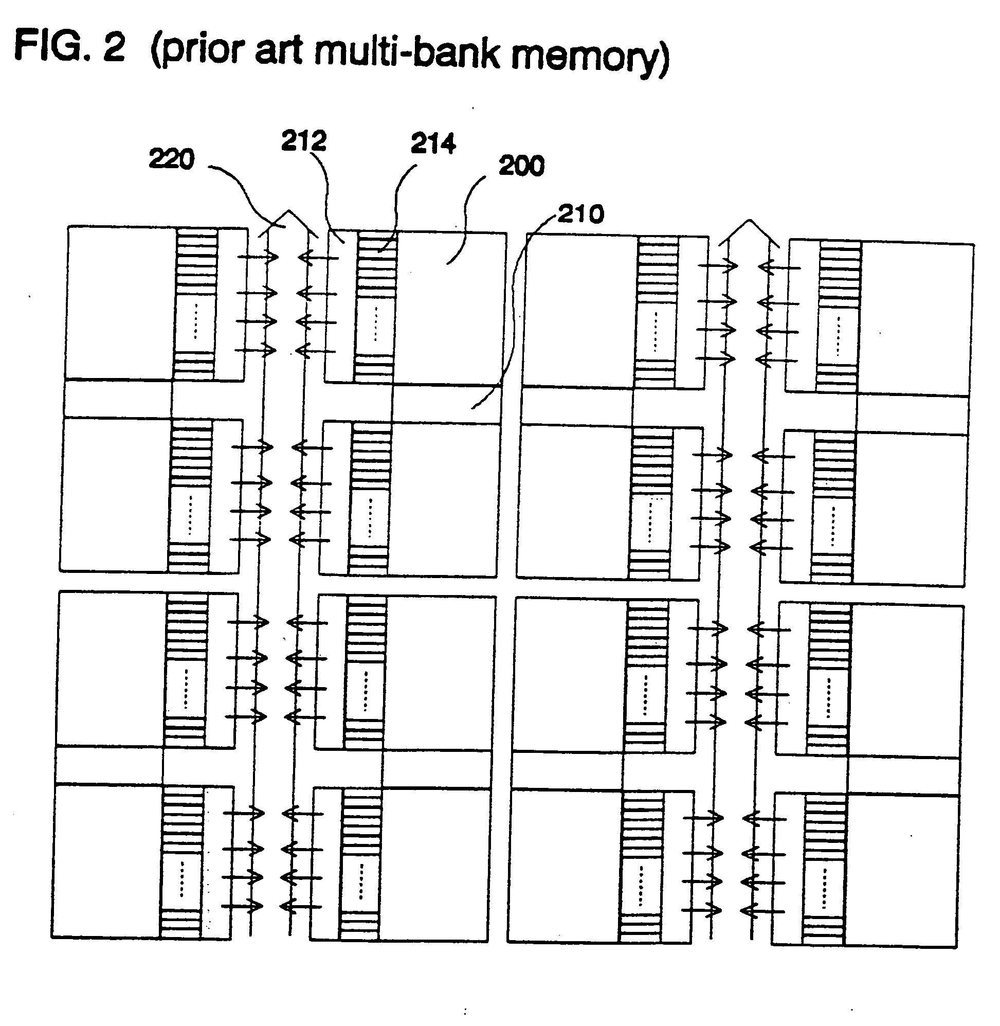
Another difficulty encountered by those of ordinary skill in the art is a limitation that Dynamic Random Access Memory (DRAM) which is usually considered as a high density, low cost, and low performance memory device cannot be conveniently integrated as embedded memory.
The major challenge to manufacture high density embedded memory is the difficulty in integrating two types of contradicting manufacture technologies together.
It is extremely difficult to have reasonable yield and reliability from such complex technology of current art.
Further more, the current art embedded technology tend to have poor performance due to contradicting requirements between logic circuits and memory devices.
None of current art embedded memory technology is proven successful.

Method used


Image

  • High performance embedded semiconductor memory devices with multiple dimension first-level bit-lines
  • High performance embedded semiconductor memory devices with multiple dimension first-level bit-lines
  • High performance embedded semiconductor memory devices with multiple dimension first-level bit-lines

Examples


Embodiment Construction

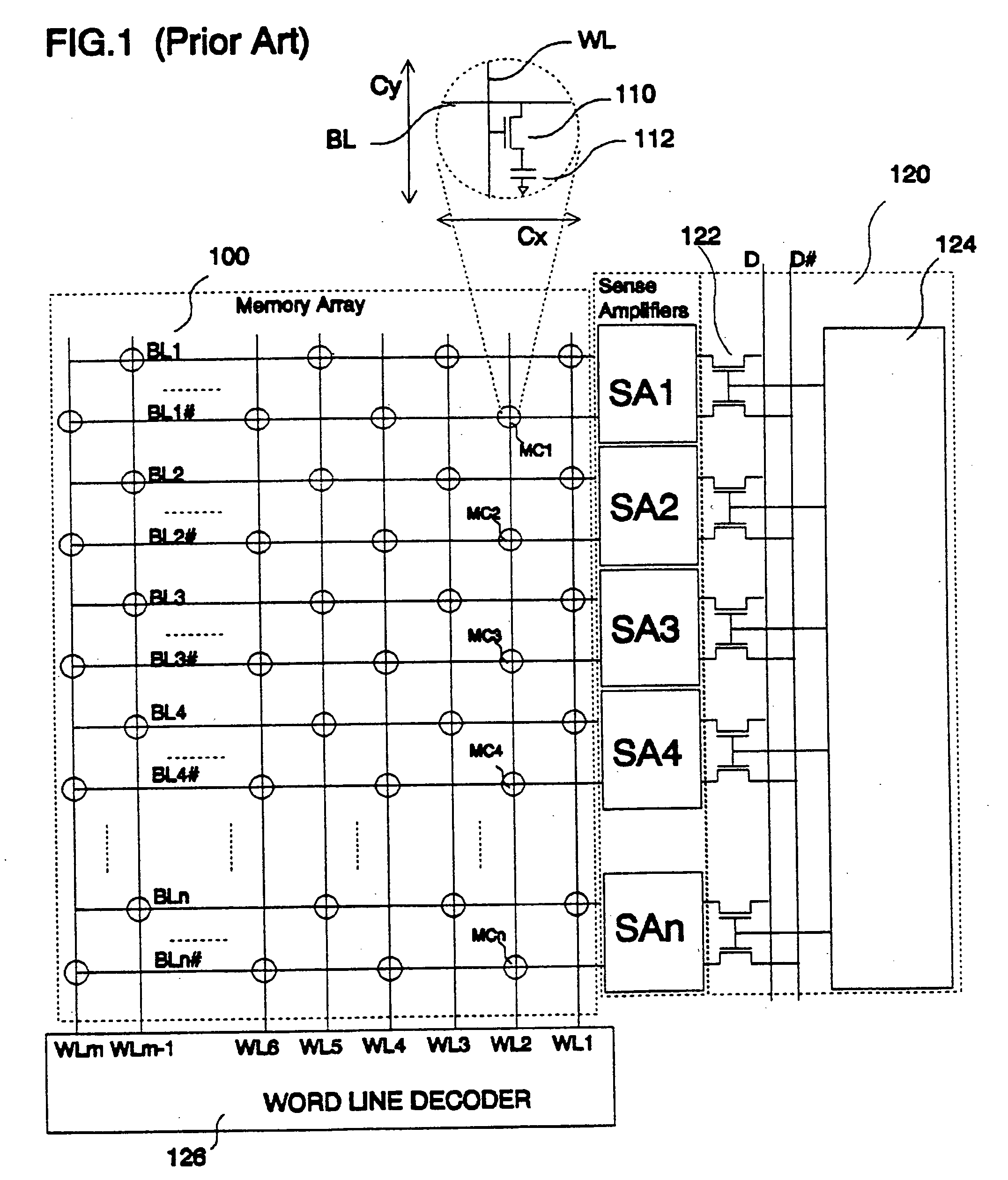
Before the invention itself is explained, a prior art semiconductor memory-device is first explained to facilitate the understanding of the invention.

FIG. 1 shows memory cell array structure of a prior art DRAM in both electrical and topographical manners. Memory cell array 100 includes plural pairs of bit lines BL1, BL1#; BL2, BL2#, BL3, BL3#; . . . ; BLn, BLn# (n; integer) which are disposed in parallel manner and a plurality of word lines WL1, WL2 . . . WLm (m; integer) which are disposed in parallel manner and also in such manner that they intersect with bit lines perpendicularly. At intersecting points, memory cells MC1, MC2, . . . , MCn are disposed. Memory cells are shown by circle marks in memory cell array 100 in FIG. 1. Each memory cell includes a switching field effect transistor 110 and memory cell capacitor 112. Bit line BL is connected to the drain of the transistor 110. The gate of transistor 110 is connected to word line WL. Sense amplifiers SA1, SA2, . . . SAn are...


PUM


Abstract

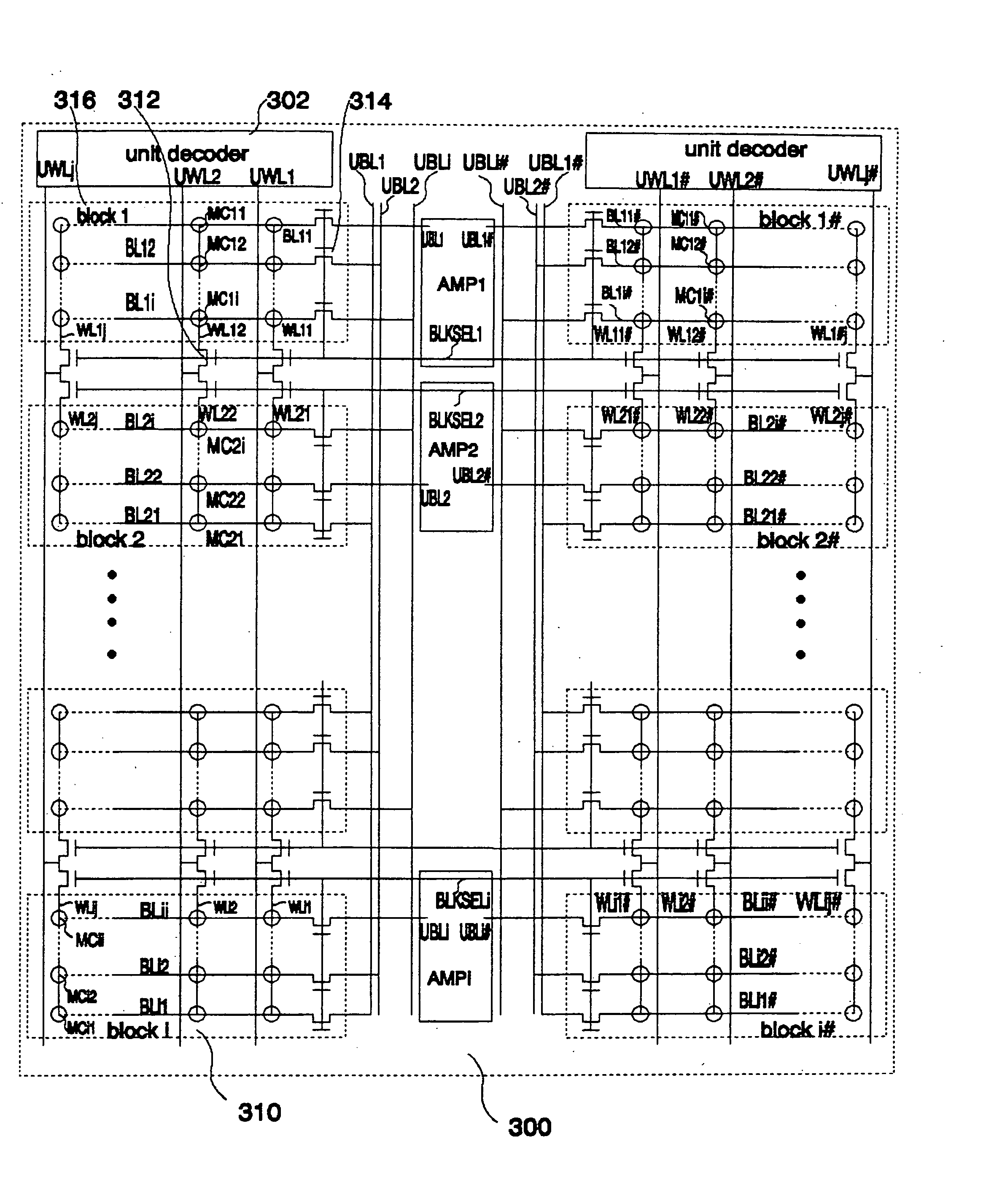
A dynamic random access memory solves long-existing tight pitch layout problems using a multiple-dimensional bit line structure. Improvement in decoder design further reduces total area of this memory. A novel memory access procedure provides the capability to make internal memory refresh completely invisible to external users. By use of such memory architecture, higher performance DRAM can be realized without degrading memory density. The requirements for system support are also simplified significantly.

Description

BACKGROUND OF THE INVENTION 1. Field of the Invention The present invention relates to high performance semiconductor memory devices, and more particularly to embedded memory devices having first level bit lines connected along different layout directions. 2. Description of the Prior Art DRAM is usually considered as a high density, low cost, but low performance memory device. DRAM's of current art always have lower performance relative to other types of semiconductor memories such as static random access memory (SRAM). The density of DRAM has been improved rapidly; the extent of integration has been more than doubled for every generation. Such higher integration of DRAM has been realized mainly by super fine processing technique and improvements in memory cell structure. In the mean time, the improvement in DRAM performance is progressing at a much slower rate. This relatively slower improvement rate in performance generates a performance gap between logic devices and memory de...

Claims


Application Information

Patent Timeline
Patent Type & Authority Applications(United States)
IPC IPC(8): G11C7/10G11C7/18G11C8/12G11C11/406G11C11/4091G11C11/4096G11C11/4097H10B12/00
CPCG11C7/1006G11C7/18G11C8/12G11C11/406H01L27/10897G11C11/4096G11C11/4097H01L27/10829G11C11/4091H10B12/37H10B12/50
Inventor SHAU, JENG-JYE
Owner UNIRAM TECH
Learn More