
Method of fabricating semiconductor device

a technology of semiconductor devices and fets, which is applied in the direction of semiconductor devices, basic electric elements, electrical equipment, etc., can solve the problems of low reliability of power transistors, variation of threshold voltages of misfets, and inability to provide fet characteristics stably with good reproducibility, so as to improve the reliability of semiconductor devices, stable fet characteristics, and good reproducibility

Inactive Publication Date: 2005-02-17
RENESAS ELECTRONICS CORP
View PDF23 Cites 7 Cited by
  • Summary
  • Abstract
  • Description
  • Claims
  • Application Information

AI Technical Summary

Benefits of technology

The present invention aims to improve the reliability of a semiconductor device and provide stable FET characteristics with good reproducibility. The invention provides a method of fabricating a semiconductor device with a MISFET of trench gate structure that prevents impurities in the semiconductor region from entering the thermal oxide film, which serves as the gate insulating film, and suppresses the degradation of the breakdown voltage of the gate insulating film. This improves the reliability of the semiconductor device and ensures stable FET characteristics with good reproducibility.

Problems solved by technology

Therefore, impurities in the p-type semiconductor region (for example, boron (B)) or impurities of the n+-type semiconductor region (for example, arsenic (As)) is introduced into the thermal oxide film and the breakdown voltage of the gate insulating film becomes easily degraded, so that the reliability of the power transistor lowers.
Further, impurities in the p-type semiconductor region at the side surface of the trench migrate into the thermal oxide film and a variation occurs in the impurity concentration in the channel forming region at the side surface of the trench, so that a variation occurs in the threshold voltage (Vth) of the MISFET and FET characteristics cannot be provided stably with good reproducibilty.

Method used


Image

  • Method of fabricating semiconductor device
  • Method of fabricating semiconductor device
  • Method of fabricating semiconductor device

Examples


first embodiment

[0050] (First Embodiment)

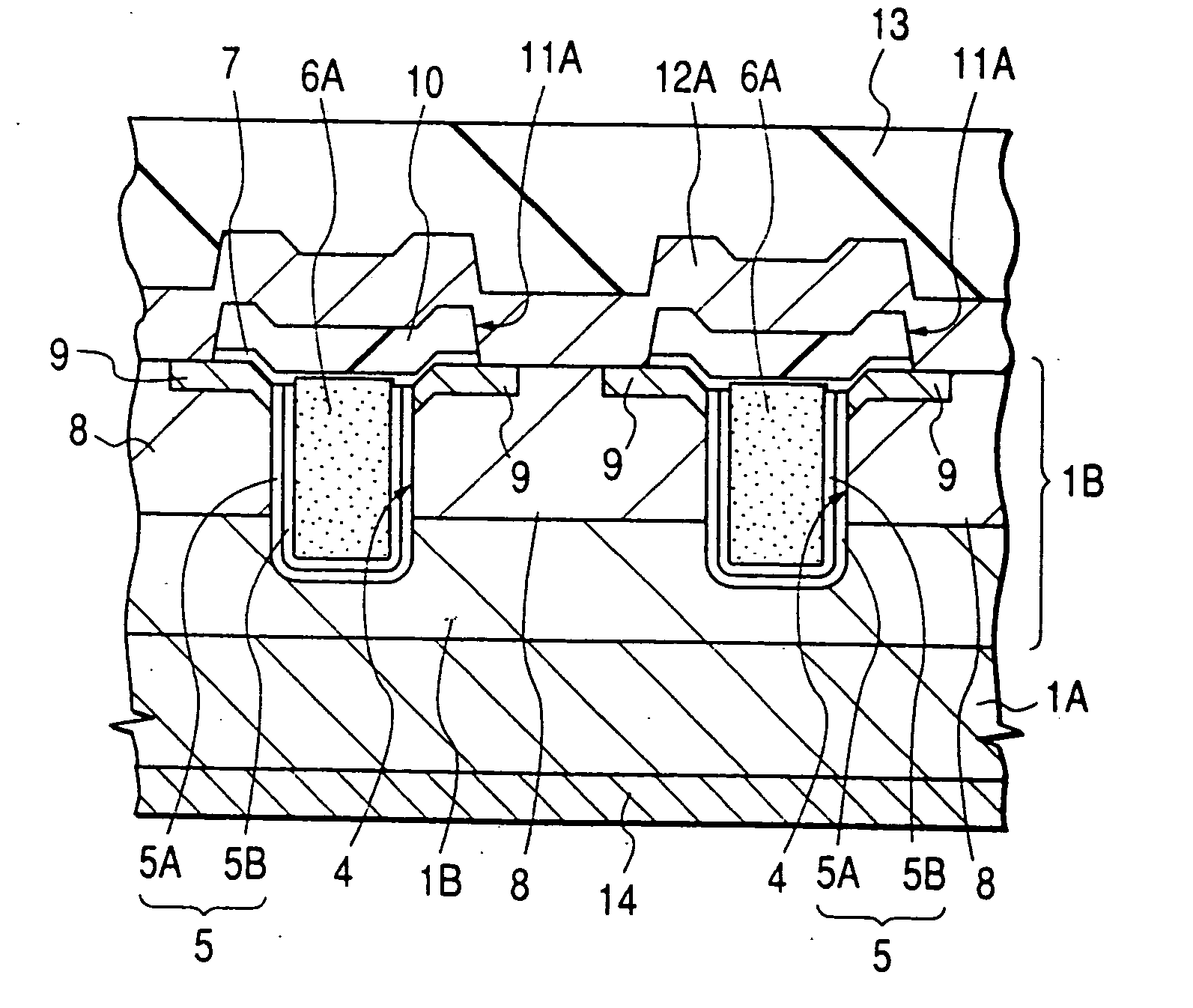
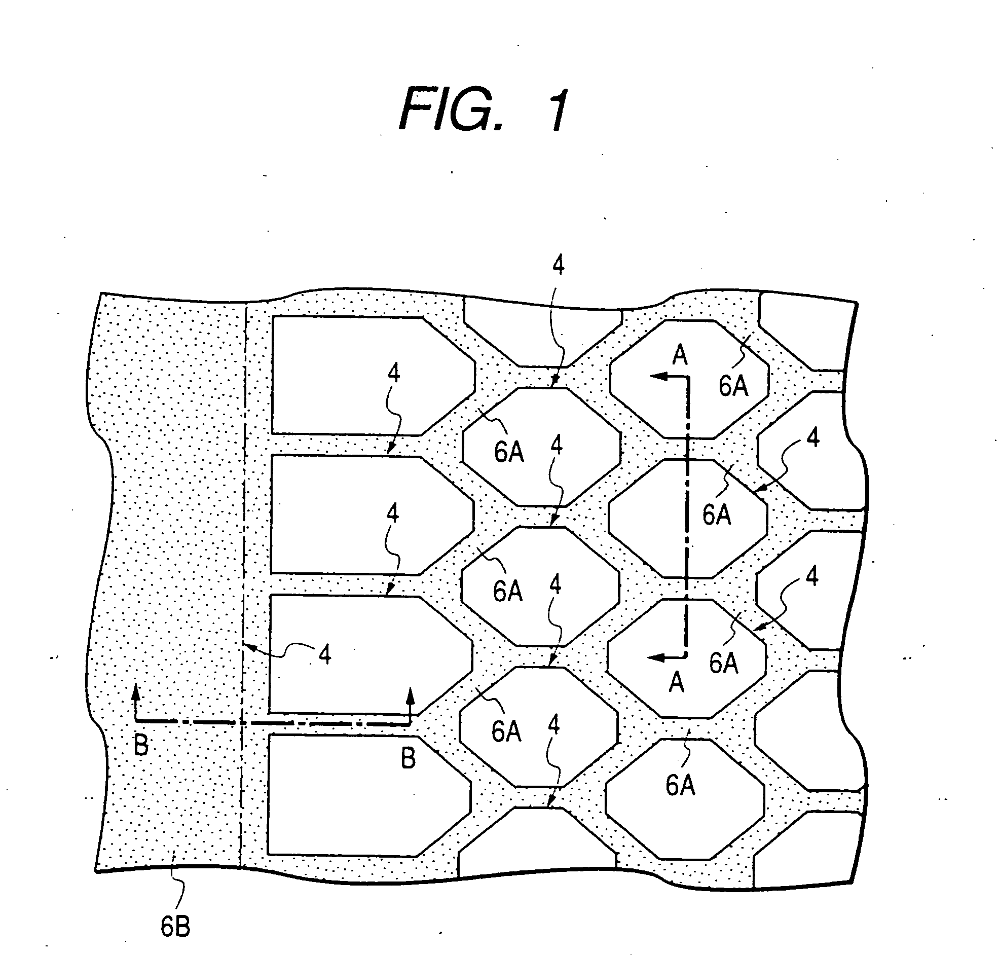
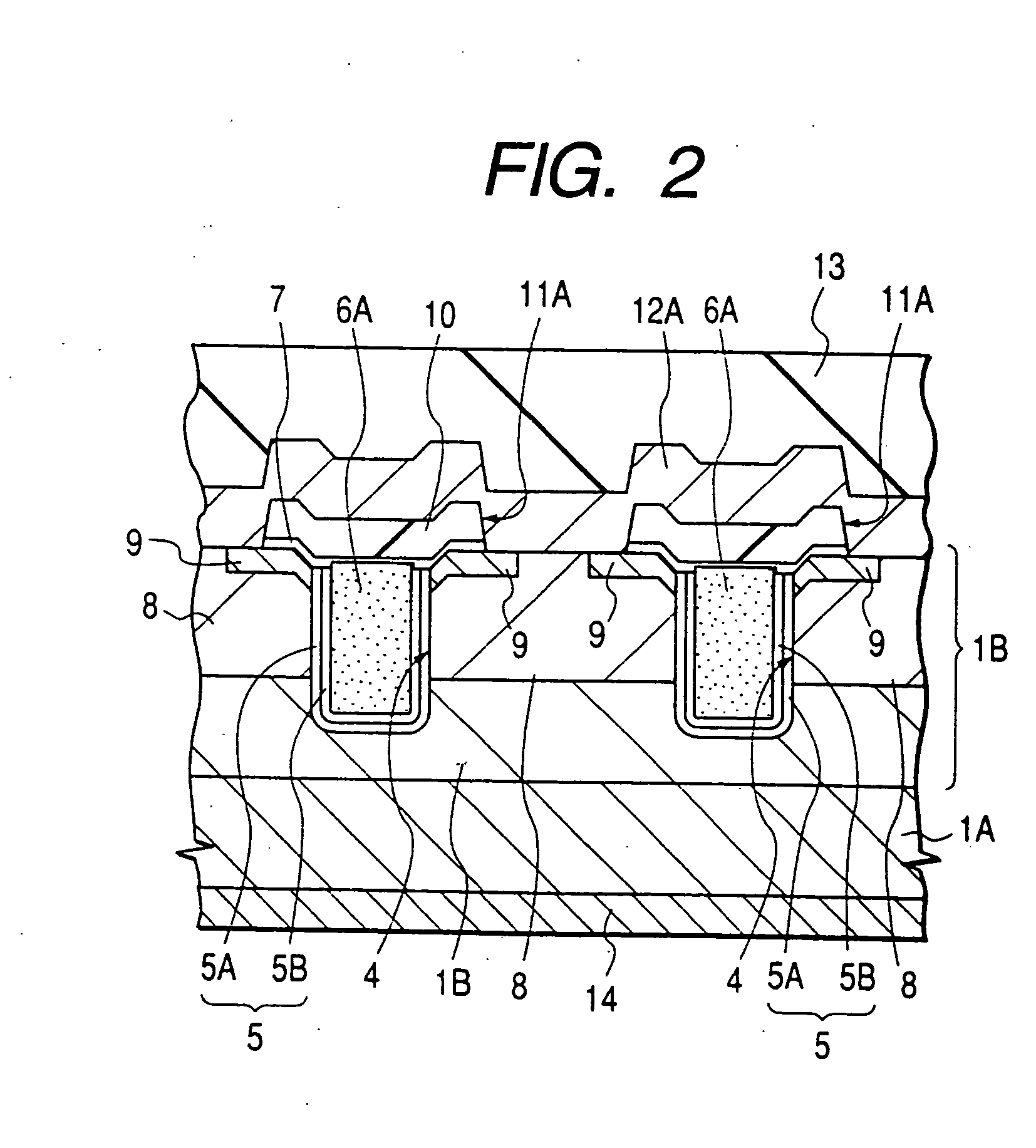
[0051]FIG. 1 is a plan view showing the essential portion of a power transistor (semiconductor device) of a first embodiment according to the present invention. FIG. 2 is a cross-sectional view taken along the line A-A shown in FIG. 1, and FIG. 3 is a cross-sectional view taken along the line B-B shown in FIG. 1. In FIG. 1, a source interconnection 12A, a gate interconnection 12B, a final passivation film 13 and the like, all of which will be described later, are not shown for the sake of-simplicity of illustration. In FIGS. 2 and 3, hatching (slant lines) indicative of a cross section is partly omitted for the sake of simplicity of illustration.

[0052] As shown in FIGS. 1 and 2, the power transistor of the first embodiment includes as its principal body a semiconductor base in which, for example, an n−-type semiconductor layer 1B is formed over a major surface of an n+-type semiconductor substrate 1A made of single-crystal silicon. The n−-type semiconductor...

second embodiment

[0092] (Second Embodiment)

[0093] A second embodiment will be described, taking an example in which a mask to be used as an etching mask during the formation of a trench is a multilayer film including a silicon oxide film, a silicon nitride film and a silicon oxide film. The reason why the mask is such multilayer film is that if the mask to be used as an etching mask during the formation of a trench is a single-layer film of silicon oxide as in the first embodiment, a hydrofluoric acid-containing etchant needs to be used for removing a reactive deposit produced during anisotropic etching and, at this time, if the film thickness of the mask 2 shown in FIG. 6 is excessively thin, the mask 2 is removed after the etching, and the process of forming the top edge portion of the trench into a gently-sloping shape by isotropic etching cannot be carried out.

[0094] In addition, under particular conditions of anisotropic etching, since reactive deposit is produced as a thin layer over the side...


PUM


Abstract

In a method of fabricating a semiconductor device having a MISFET of trench gate structure, a trench is formed from a major surface of a semiconductor layer of first conductivity type which serves as a drain region, in a depth direction of the semiconductor layer, a gate insulating film including a thermal oxide film and a deposited film is formed over the internal surface of the trench, and after a gate electrode has been formed in the trench, impurities are introduced into the semiconductor substrate of first conductivity type to form a semiconductor region of second conductivity type which serves as a channel forming region, and impurities are introduced into the semiconductor region of second conductivity type to form the semiconductor region of first conductivity type which serves as a source region.

Description

FIELD OF THE INVENTION [0001] The present invention relates to a semiconductor device and, more particularly, to an art which can be usefully applied to a semiconductor device having a transistor element of trench gate structure. BACKGROUND OF THE INVENTION [0002] Power transistors (semiconductor devices) are used as switching elements for power amplification circuits, power supply circuits and the like. This kind of power transistors has a construction in which a plurality of transistor elements are electrically connected in parallel. Each of the transistor elements is constructed as, for example, a MISFET (Metal Insulator Semiconductor Field Effect Transistor) of trench gate structure. A method of fabricating a power transistor having a MISFET of trench gate structure will be described below. [0003] First, an n−-type semiconductor layer is formed over a major surface of an n+-type semiconductor substrate made of single-crystal silicon by an epitaxial growth method. These n+-type s...

Claims


Application Information

Patent Timeline
Patent Type & Authority Applications(United States)
IPC IPC(8): H01L21/28H01L21/336H01L29/423H01L29/51H01L29/78
CPCH01L21/28185H01L29/7827H01L21/28202H01L21/28211H01L29/0696H01L29/0869H01L29/4236H01L29/42376H01L29/4238H01L29/511H01L29/513H01L29/518H01L29/66734H01L29/7813H01L21/28114H01L29/66666H01L21/28194
Inventor NUMAZAWA, SUMITONAKAZAWA, YOSHITOKOBAYASHI, MASAYOSHIKUDO, SATOSHIIMAI, YASUOKUBO, SAKAESHIGEMATSU, TAKASHIOHNISHI, AKIHIROUESAWA, KOZOOISHI, KENTARO
Owner RENESAS ELECTRONICS CORP
Learn More