Semiconductor device including a capacitor having improved structural stability and enhanced capacitance, and method of manufacturing the semiconductor device

a semiconductor and capacitor technology, applied in the direction of semiconductor devices, capacitors, electrical equipment, etc., can solve the problems of insufficient affecting the stability of semiconductor devices, and affecting the operation of semiconductor memory devices, so as to improve the reliability, improve the structural stability, and improve the effect of the semiconductor manufacturing process

Active Publication Date: 2005-02-24
SAMSUNG ELECTRONICS CO LTD
View PDF14 Cites 26 Cited by
  • Summary
  • Abstract
  • Description
  • Claims
  • Application Information

AI Technical Summary

Benefits of technology

[0033] According to the present invention, the stabilizing members are formed to encompass the upper portions of the cylindrical storage electrodes so that the storage electrodes of a unit memory cell are supported by one another. Thus, the capacitors including the storage electrode and the stabilizing members may have improved structural stability even when the capacitors have an extremely high aspect ratio. As a result, a semiconductor device including the capacitors may have improved reliability and the throughput of a semiconductor manufacturing process may be increased. Meanwhile, since the stabilizing members are formed using material that is highly resistant to the LAL solution, or the protecting members enclosing the stabilizing members are formed using metal oxide that is highly resistant to the LAL solution, the storage electrodes may more stably support one another by interposing the stabilizing members, thereby greatly increasing the structural stability of the capacitors. In addition, the capacitors may have primarily improved capacitance because the stabilizing members having extended bowl structures or ring structures may enlarge the area of the storage electrodes. Furthermore, the storage electrodes are formed on sidewalls of the contact holes having an extended area by the cleaning process so that the storage electrodes have a secondarily enlarged area. As a result, the capacitors including the storage electrodes may have greatly improved capacitance.

Problems solved by technology

However, due to design constraints of the semiconductor memory device that include size decreases, the capacitor should have an increasingly large aspect ratio, defined as the ratio between the height and width of the capacitor.
As a result, however, the capacitors having a high aspect ratio may mechanically collapse so that a so-called two-bit failure may occur between adjacent capacitors.
When the cylindrical storage electrode has this greatly increased height, the cylindrical storage electrode may collapse toward an adjacent cylindrical electrode so that adjacent capacitors may be inadvertently connected to each other.
When the two-bit failure occurs in the semiconductor memory device, the semiconductor memory device may not properly operate.
However, in the above-described semiconductor device, processes for manufacturing the semiconductor device are complicated because at least four beam-shaped insulating members 130 should be formed between the adjacent bottom electrodes 105 in order to improve the mechanical strength of the capacitor 120.
Thus, manufacturing cost and manufacturing time for the semiconductor device is increased.
As a result, the processes for manufacturing the semiconductor device including the capacitor 120 having the complex structure may have poor throughput.

Method used


Image

  • Semiconductor device including a capacitor having improved structural stability and enhanced capacitance, and method of manufacturing the semiconductor device
  • Semiconductor device including a capacitor having improved structural stability and enhanced capacitance, and method of manufacturing the semiconductor device
  • Semiconductor device including a capacitor having improved structural stability and enhanced capacitance, and method of manufacturing the semiconductor device

Examples


Embodiment Construction

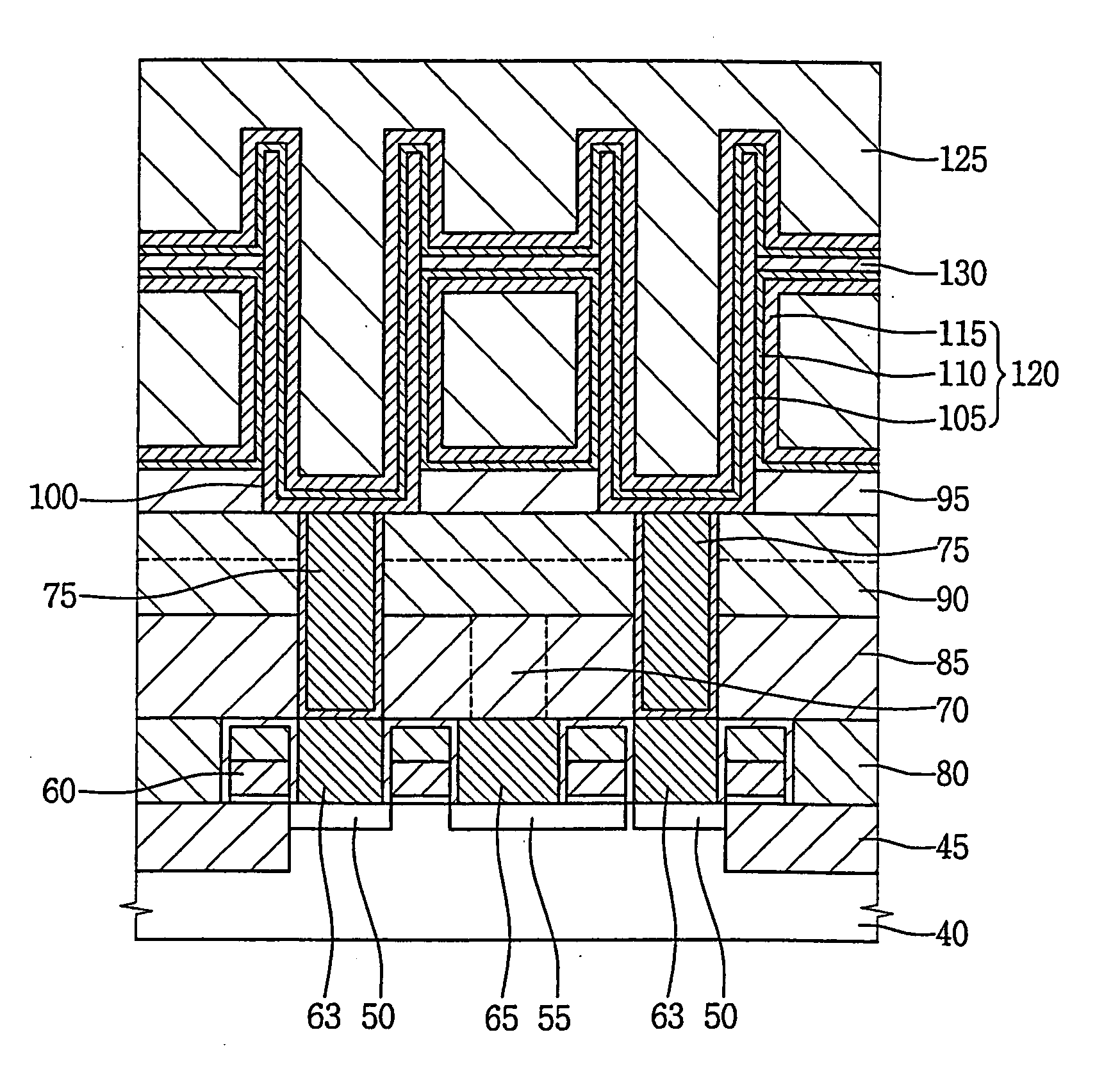
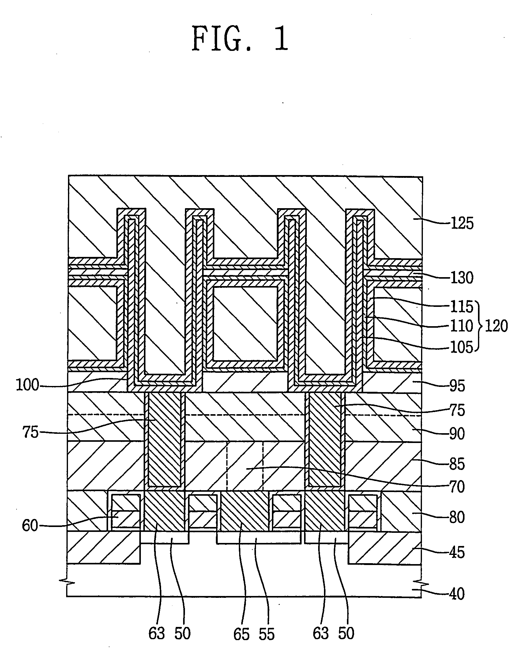
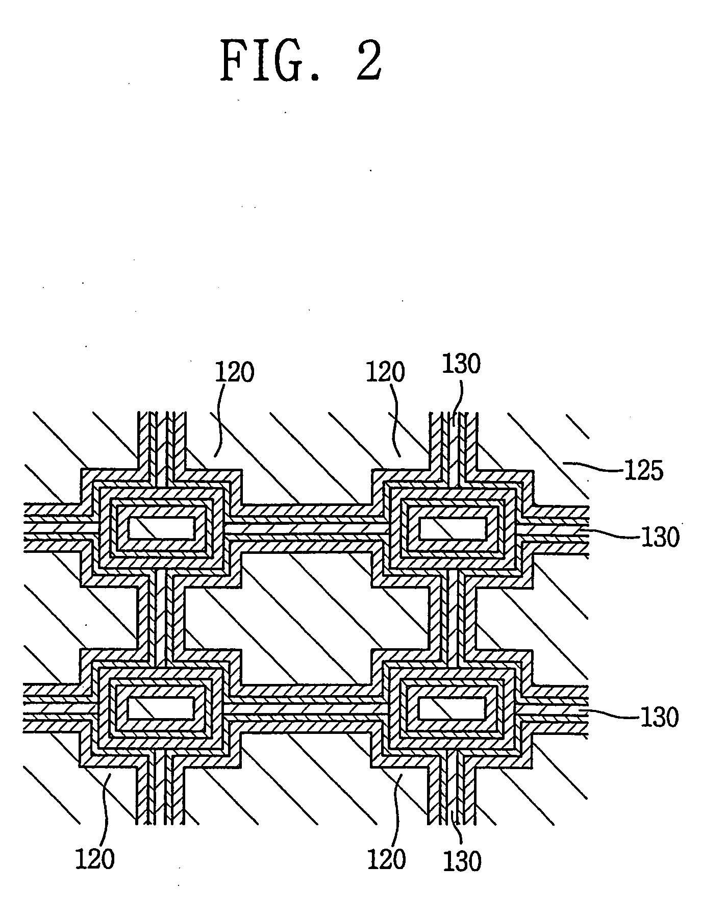
[0044] The present invention now will be described more fully hereinafter with reference to the accompanying drawings, in which embodiments of the invention are shown In the drawings, the thickness of layers and regions are exaggerated for clarity. Like reference numerals refer to similar or identical elements throughout. It will be understood that when an element such as a layer, a region or a substrate is referred to as being “on” or “onto” another element, it can be directly on the other element or intervening elements may also be present.

[0045]FIGS. 3 and 4 are cross-sectional views illustrating steps for forming first pads 250 and second pads 255 on a semiconductor substrate 200 including word lines 233.

[0046] Referring to FIGS. 3 and 4, the semiconductor substrate 200 is divided into an active region and a field region by forming an isolation layer 205 at surface portions of the semiconductor substrate 200. The isolation layer 205 may be formed by a shallow trench isolation ...


PUM


Abstract

In a method of manufacturing a semiconductor device including a capacitor having improved structural stability and enhanced capacitance, a contact region is formed on a surface portion of a semiconductor substrate. After a mold layer is formed on the substrate, a stabilizing member is formed to encompass a storage electrode. A contact hole is formed through the mold layer to expose a sidewall of the stabilizing member and the contact region. The storage electrode is formed on the exposed contact region and on the exposed sidewall of the stabilizing member. A dielectric layer and a plate electrode are successively formed on the storage electrode. The capacitor including the storage electrode and the stabilizing member will have improved structural stability that resists mechanical collapse even when the capacitor has an extremely high aspect ratio.

Description

CROSS REFERENCE TO RELATED APPLICATION [0001] This application claims priority under 35 USC §119 to Korean Patent Application No. 2003-56959 filed on Aug. 18, 2003, the content of which is incorporated herein by reference in its entirety. BACKGROUND OF THE INVENTION [0002] 1. Field of the Invention [0003] The present invention relates to a semiconductor device and a method of manufacturing the semiconductor device. More particularly, the present invention relates to a semiconductor device including an improved structural stability and an enhanced capacitance, and a method of manufacturing the semiconductor device. [0004] 2. Description of the Related Art [0005] In general, semiconductor memory devices such as dynamic random access memory (DRAM) devices or static random access memory (SRAM) devices can store data or information therein. The data or information is stored in the semiconductor memory devices, and also the data or information is read from the semiconductor memory devices...

Claims


Application Information

Patent Timeline
Patent Type & Authority Applications(United States)
IPC IPC(8): H01L21/02H01L21/768H01L21/311H01L21/3213H01L21/8242H01L27/02H01L27/108
CPCH01L21/02063H01L21/31116H01L21/76802H01L28/91H01L27/10814H01L27/10852H01L27/0207H10B12/315H10B12/033H10B99/00
Inventor PARK, JE-MIN
Owner SAMSUNG ELECTRONICS CO LTD
Why Eureka
Try Eureka