
Absorption current image apparatus in electron microscope

an electron microscope and current image technology, applied in the field of electron beam apparatus, can solve the problems of resolution degradation, limited structure of measurable samples, and inability to observe high-resolution samples at low acceleration, and achieve the effect of high speed and high precision

Active Publication Date: 2005-03-03
HITACHI HIGH-TECH CORP
View PDF3 Cites 21 Cited by
  • Summary
  • Abstract
  • Description
  • Claims
  • Application Information

AI Technical Summary

Benefits of technology

Through the use of the present invention, absorption current measurement can be performed at a high speed and with a high precision and, thus, the invention is very useful for use in semiconductor inspection equipment.
It becomes possible to observe even wet samples and samples vulnerable to electron bombardment at a high resolution in a low vacuum atmosphere.

Problems solved by technology

In this respect, in the prior art absorption current measurement method, measurable samples are limited in structure; i.e., an insulative substrate and a substrate with an oxide film on the back for which accurate absorption current frequency characteristic measurements cannot be performed.
In the prior art example, a retarding method which decelerates an incident electron beam by applying a high voltage to the substrate cannot be used because the sample and the current measuring circuit are directly connected, and there was a problem that high-resolution observation is impossible at low acceleration.
This is because, in a low acceleration region, a chromatic aberration of an objective lens becomes large, which results in resolution degradation.
This posed a problem that high-speed measurement is hard to do.

Method used


Image

  • Absorption current image apparatus in electron microscope
  • Absorption current image apparatus in electron microscope
  • Absorption current image apparatus in electron microscope

Examples


embodiment 1

[Embodiment 1]

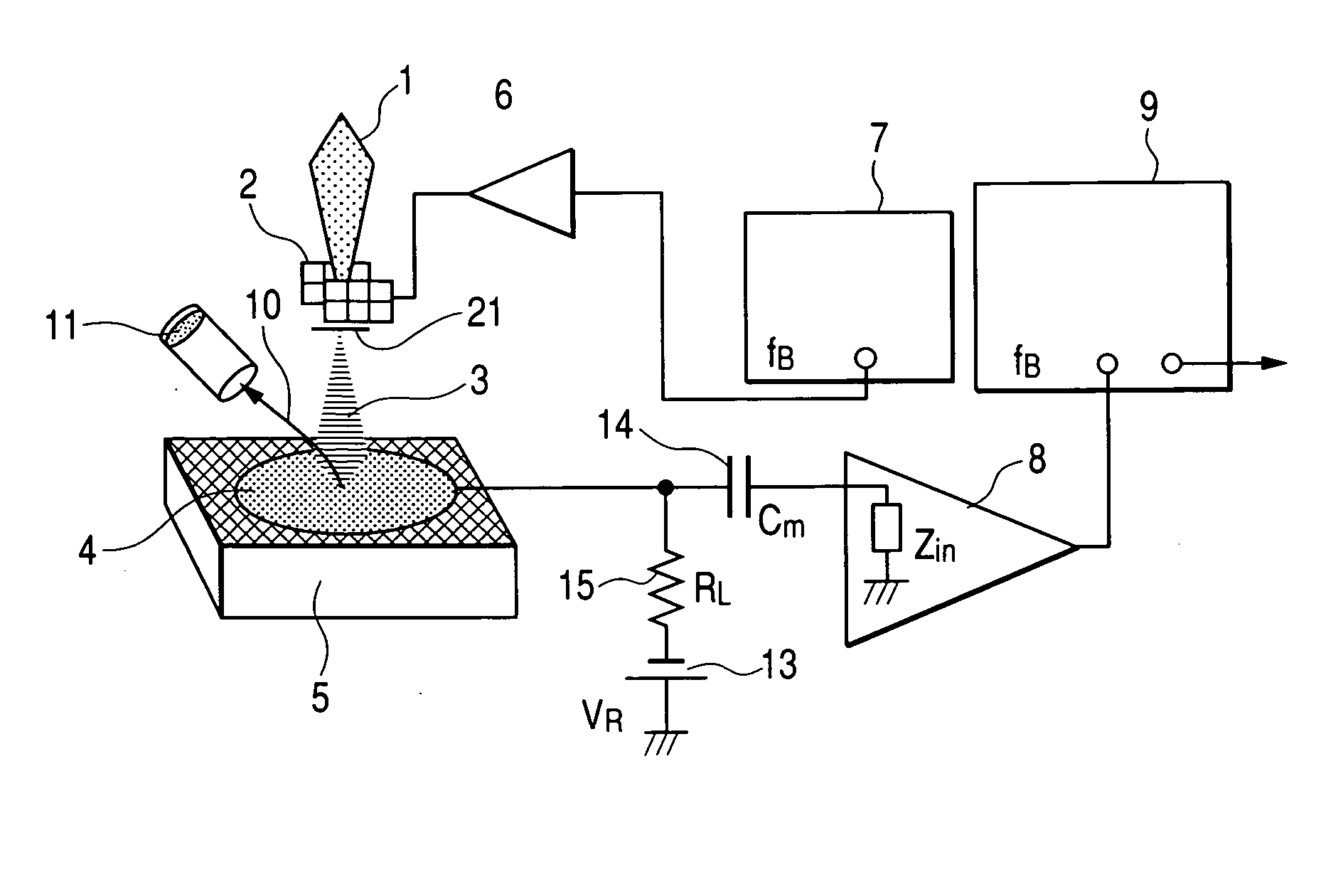
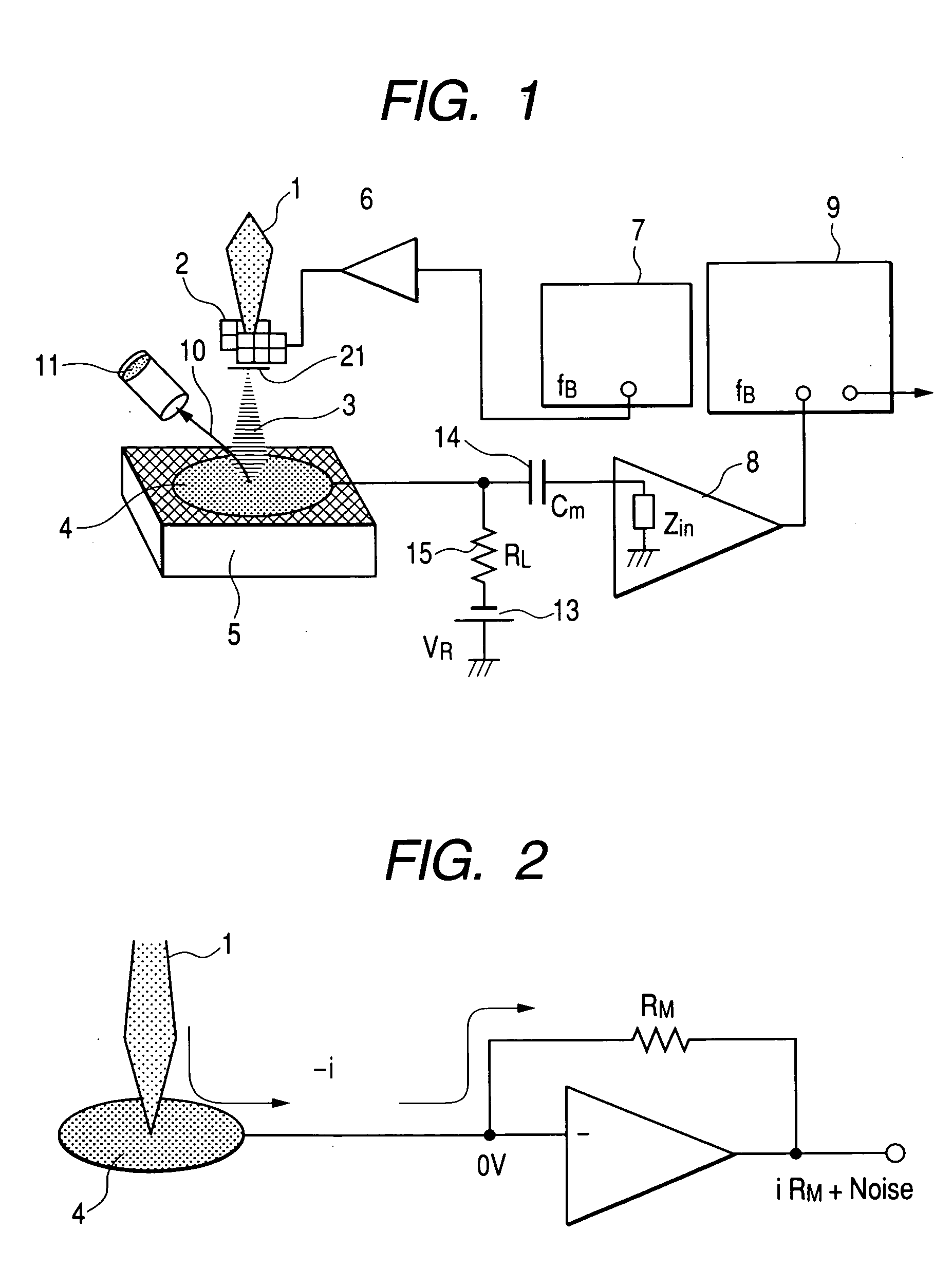
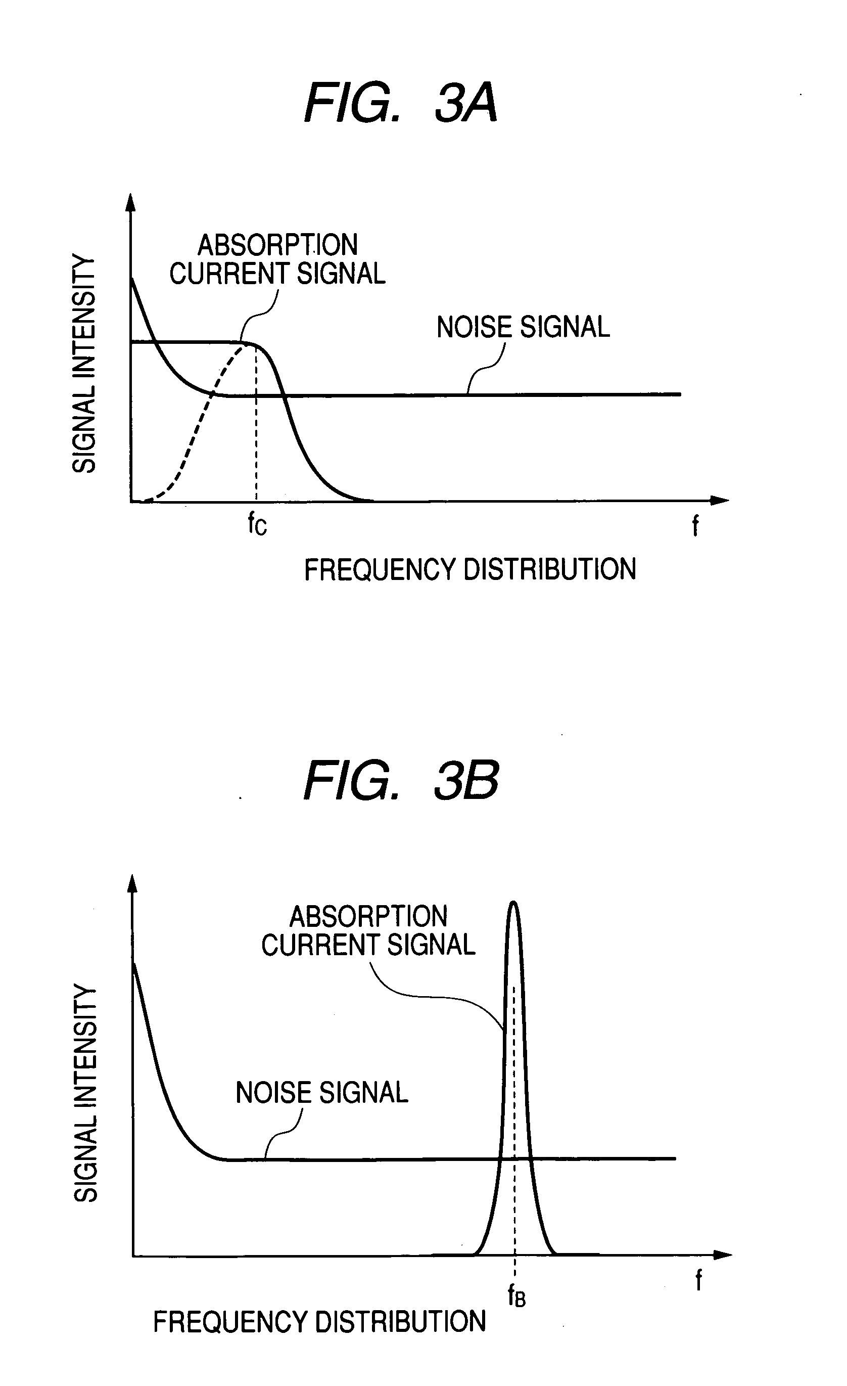
FIG. 1 shows a schematic of SEM equipment according a preferred Embodiment 1 of the invention. In the scanning electron microscope (SEM) equipment, a continuous electron beam 1 is produced and converted to a pulse electron beam 3 through blanking electrodes 2 and a blanking slit 21 located in the beam passage. The blanking electrodes 2 are flat parallel and a pulsing voltage generated by a blanking amplifier 6 is applied to one of the electrodes with the other serving as a ground electrode or inverse voltages are applied to both the electrodes. The voltage to be applied is determined by acceleration voltage and an electric field produced between the blanking electrodes 2, which is conditioned that the voltage application causes the electron beam to bend, and hence the beam cannot pass the slit 21. A pulse cycle is determined by-a pulse generator 7 and a pulse voltage generated by the pulse generator is amplified by the blanking amplifier 6 and applied to-the blanking e...

embodiment 2

[Embodiment 2]

FIG. 6 shows a schematic of SEM equipment according a preferred Embodiment 2 of the invention. This SEM is intended to inspect semiconductor wafers as samples with an acceleration voltage decreased to the order of 1 kV for measurement with a low possibility of damaging the sample under inspection. An electron source 22 is a diffusion-supply-type electron source using Zr / O / W and, by application of an extraction voltage V1 between extractor electrodes 23 and itself, generates a continuous electron beam 1 with electronic energy V0. An electron source controller 24 exerts control of the electron source and communicates information with a SEM controller 25. The lens action a condenser lens 27 focuses the continuous electron beam 1 around blanking slits 21. To blanking electrodes 2, a blanking voltage is applied and this voltage is an intended voltage to which a blanking amplifier converts pulses generated by a pulse generator 7. Information such as blanking frequency fB and...

embodiment 3

[Embodiment 3]

FIG. 11 is a schematic diagram of SEM equipment according a preferred Embodiment 3 of the invention. The SEM equipment of Embodiment 3 which is provided as an absorption current image apparatus is intended to observe samples in a low vacuum atmosphere, which is suitable for observing wet-organic matters such as living bodies and protein or semiconductor samples. In Embodiment 3, the pressure of a vacuum sample chamber ranging from 270 Pa to atmospheric pressure is referred to as low vacuum. Acceleration voltage falls between 1 kV and 30 kV.

Absorption current measurements are not affected by the degree of vacuum even in the prior art method thereof. However, absorption current measurements in a low vacuum environment are not practical, because of low sensitivity and time consumption. In such an environment, mainly, measurements were taken for back scattered electrons. In this case, because back scattered electrons are lost when they collide with gas in the sample cham...


PUM


Abstract

It was hard for conventional SEMs to take measurements at a high speed and take accurate measurements when an insulator exists between an object to probe and the detector, because the conventional SEMs used a continuous electron beam. Also, it was impossible to apply voltage to the sample during the measurement of current. By pulse-modulating the electron beam and extracting a high-frequency signal component from the sample, new SEM equipment disclosed herein detects electrons absorbed in the sample at a high speed and with precision. Precise and high-speed absorption current measurements can be achieved. High-functionality inspection apparatus can be provided.

Description

CLAIM OF PRIORITY The present invention claims priority from Japanese application JP 2003-299477 filed on Aug. 25, 2003, the content of which is hereby incorporated by reference on to this application. BACKGROUND OF THE INVENTION The present invention relates to an electron beam apparatus and, more particularly, to an absorption current image measurement apparatus suitable for sample measurement and inspection with an electron microscope. In scanning electron microscope (SEM) inspection using an electron beam in a semiconductor process, essentially, measurements are taken for secondary electrons from a sample. However, a problem was presented that, for deep holes and trenches with a narrow width or samples with a nonuniformly charged surface, secondary electrons from the surface irradiated with a probe electron beam cannot be measured sufficiently. As prior art means to solve this problem, for example, there is a sample measurement method using absorption current, K. Yamada, et a...

Claims


Application Information

Patent Timeline
IPC IPC(8): G01N23/225G01Q30/02H01J37/04H01J37/244H01J37/28
CPCH01J37/244H01J2237/2605H01J37/28
Inventor OHSHIMA, TAKASHIMAKINO, HIROSHITOYAMA, HIROSHISHINADA, HIROYUKI
Owner HITACHI HIGH-TECH CORP
Learn More