Electric component for communication device and semiconductor device for switching transmission and reception

a communication device and semiconductor technology, applied in the direction of gated amplifiers, emergency protective arrangements for limiting excess voltage/current, amplifier modifications to reduce non-linear distortion, etc., can solve the problems of increasing the size of the module, etc., to reduce the number of components composing the system and a module, the effect of increasing the mounting density

Active Publication Date: 2005-03-03
MURATA MFG CO LTD
View PDF6 Cites 79 Cited by
  • Summary
  • Abstract
  • Description
  • Claims
  • Application Information

AI Technical Summary

Benefits of technology

[0021] With the foregoing means, the number of components composing the system and a module can be reduced and the mounting density can be increased by using the FET or FETs in place of a diode as an element composing the switch circuit. By progressively reducing the resistance values of the gate resistors in the direction from the gate to which a highest voltage is applied toward the gate to which a lowest voltage is applied, it becomes possible to circumvent the situation in which the FET to which a higher voltage is inputted is brought into the ON state earlier, reduce insertion loss, and thereby reduce harmonic distortion. By applying a dc voltage for biasing to each of the transmitter terminal and the terminal connected to the antenna, the maximum permissible power of an RF signal inputted to the transmitter terminal can be increased.

Problems solved by technology

Therefore, in a system requiring a plurality of diodes such as a quad band system, a module on which it is mounted has the problems of increased size and high current consumption particularly.
In addition to a diode element, the transmission / reception switching circuit using a diode also requires a λ / 4 microstrip line having a length of approximately 5 mm, which causes a further increase in the size of the module.
As a result, it was proved that the transmission / reception switching circuit using a FET has the following problem.

Method used


Image

  • Electric component for communication device and semiconductor device for switching transmission and reception
  • Electric component for communication device and semiconductor device for switching transmission and reception
  • Electric component for communication device and semiconductor device for switching transmission and reception

Examples


first embodiment

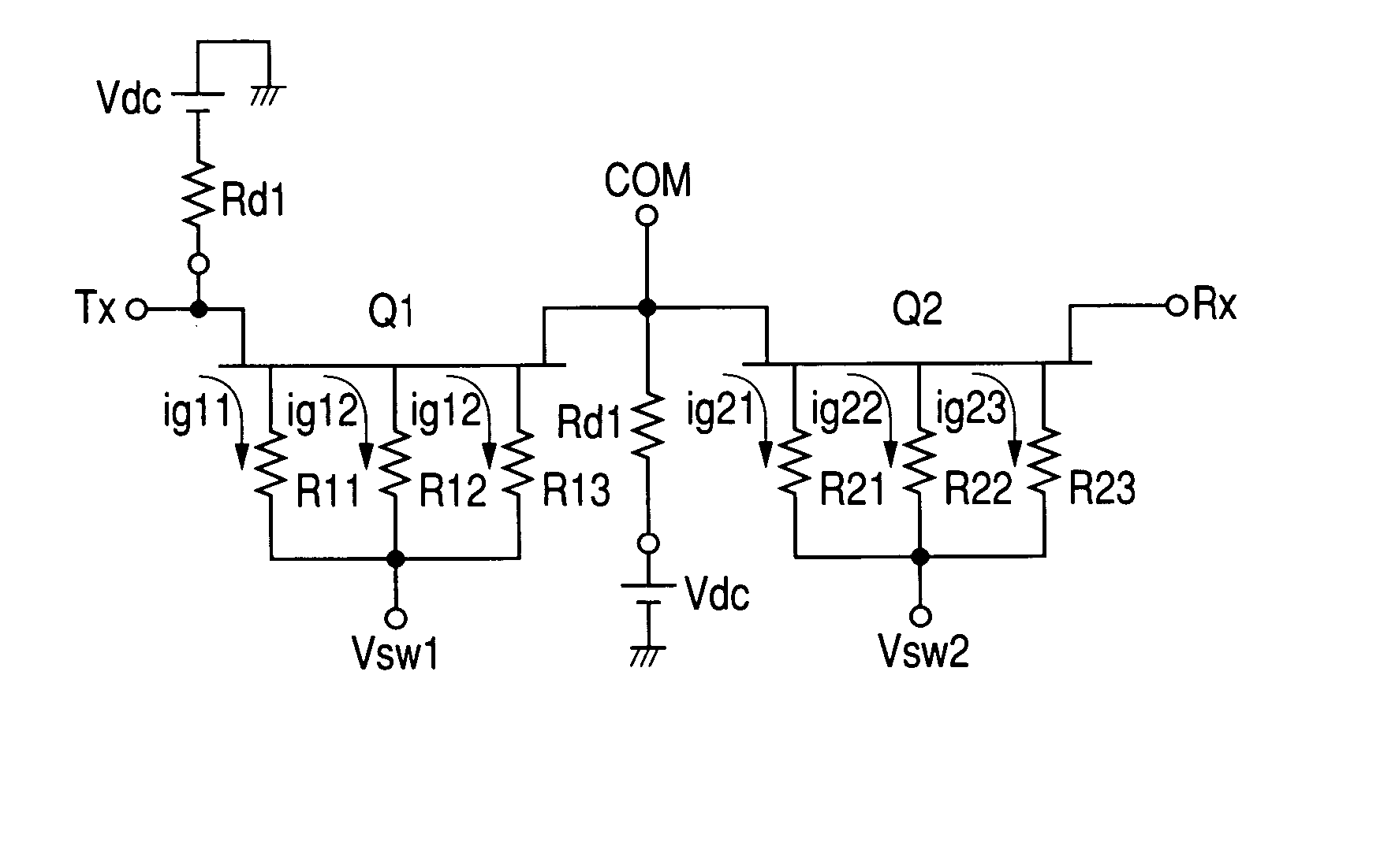
[0035]FIG. 1 shows a transmission / reception switch circuit according to the present embodiment. The transmission / reception switch circuit of the present embodiment is formed as a semiconductor integrated circuit on a semiconductor substrate such as a GaAs chip.

[0036] The transmission / reception switch circuit of the present embodiment comprises: a first switch transistor Q1 connected between a transmitter terminal Tx connected to the output terminal of a power amplifier and a common terminal COM connected to an antenna; and a second switch transistor Q2 connected between the foregoing common terminal COM and a receiver terminal Rx to which the input terminal of a receiving circuit such as a low noise amplifier is connected. A dc voltage Vdc is applied to the foregoing transmitter terminal Tx and common terminal COM via respective external resistors Rd1 and Rd2.

[0037] As the transistors Q1 and Q2, depletion-type P-channel HEMTs are used. Each of the transistors Q1 and Q2 is formed as...

third embodiment

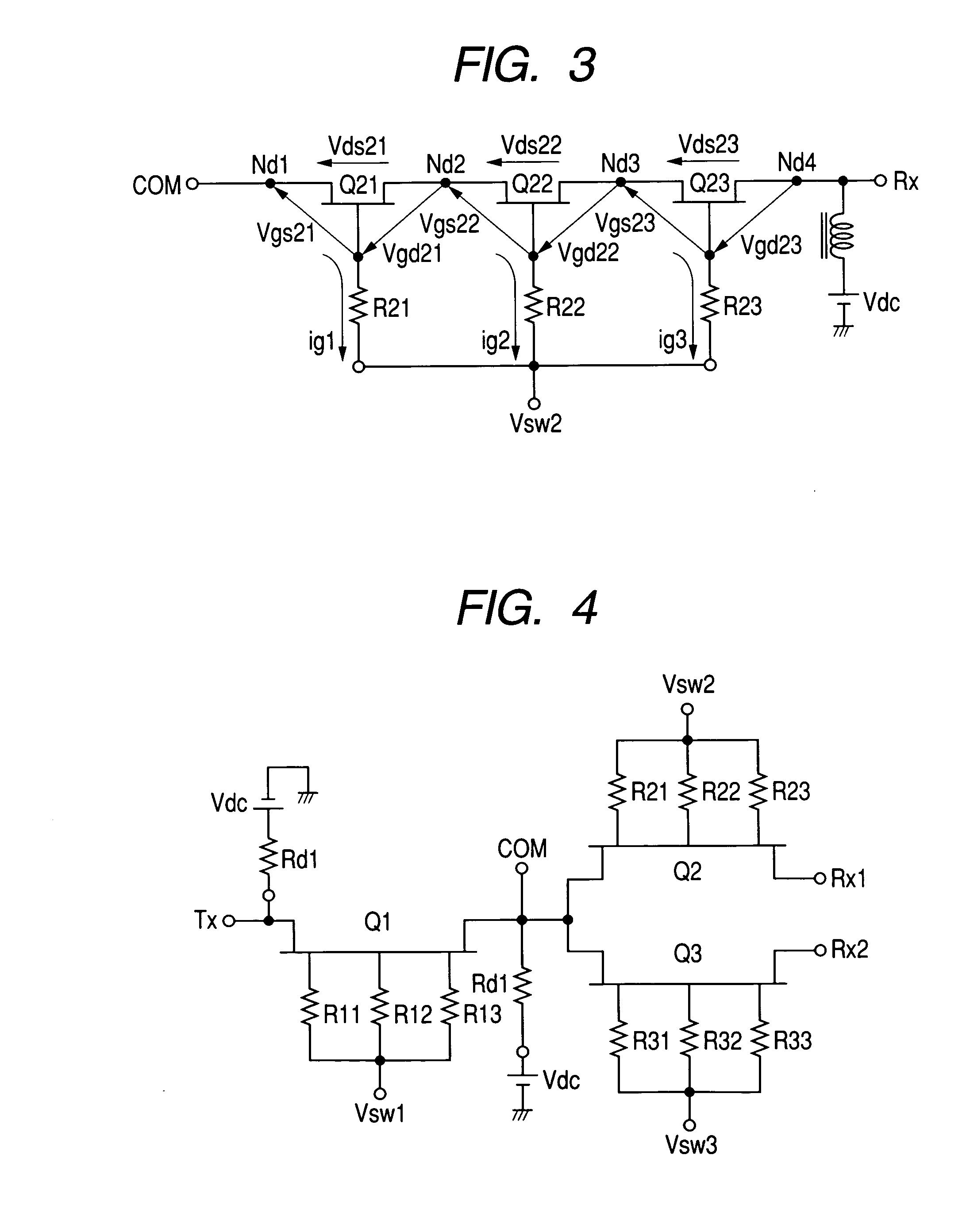
[0050]FIG. 4 shows the transmission / reception switch circuit according to the present invention.

[0051] In this embodiment, a switching transistor Q3 is provided between the common terminal COM connected to the antenna and a second receiver terminal Rx2 to be in parallel with the switching transistor Q2 in the embodiment of FIG. 1. The transistor Q3 is composed of a triple gate HEMT, similarly to the transistor Q2. The ratio among the resistance values r31, r32, and r33 of resistors R31, R32, and R33 connected to the gates has been set to 3:2:1. The switching circuit of this embodiment is used conveniently to compose a system capable of transmitting and receiving signals in two different frequency bands, such as signals in the GSM mode and signals in the DCS mode.

fourth embodiment

[0052]FIG. 5 shows the transmission / reception switch circuit according to the present invention.

[0053] In this embodiment, switching transistors Q3 and Q4 in a parallel configuration are provided between the switching transistor Q2 in the embodiment of FIG. 1 and the first receiver terminal Rx1 and between the switching transistor Q2 and the second receiver terminal Rx2 to further enhance isolation at the receiver. Each of the transistors Q3 and Q4 is composed of a double-gate HEMT. The resistance values r31, r32, r41, and r42 of the resistances R31, R32, R41, and R42 have been set to satisfy r31≧r32 and r41≧r42. The switching circuit of this embodiment is also used conveniently to compose a system capable of transmitting and receiving signals in two different frequency bands such as signals in the GSM mode and signals in the DCS mode.

[0054]FIG. 6 shows a schematic structure of a preferred embodiment of a module composed of the transmission / reception switching circuit according to ...


PUM


Abstract

There are provided a transmission/reception switching circuit which is small in insertion loss and harmonic distortion and allows an increase in the output power of a power amplifier and an electronic component for communication on which the transmission/reception switching circuit is mounted. As an element composing a transmission/reception switching circuit in a wireless communication system, series-connected FETs or a multi-gate FET are used in place of a diode. Gate resistors connected between the individual gate terminals and a control terminal are designed to have resistance values which become progressively smaller from the gate to which a highest voltage is applied toward the gate to which a lowest voltage is applied.

Description

CROSS-REFERENCE TO RELATED APPLICATION [0001] The present application claims priority from Japanese Patent Application JP 2003-208960 filed on Aug. 27, 2003, the content of which is hereby incorporated by reference into this application. BACKGROUND OF THE INVENTION [0002] The present invention relates to a technology which is effective when applied to a transmission / reception switching circuit in a wireless communication system and further to the case where isolation between an antenna and a receiver circuit is thereby improved by reducing insertion loss. More particularly, the present invention relates to a technology which is effective when applied to a semiconductor integrated circuit formed with a transmission / reception switching circuit used in, e.g., a mobile phone, to a front-end module on which the semiconductor integrated circuit, a lowpass filter, an impedance matching circuit, and the like are mounted, and further to an electronic component for communication such as a pow...

Claims


Application Information

Patent Timeline
Patent Type & Authority Applications(United States)
IPC IPC(8): H03F1/02H04B1/44H03F1/32H03F3/195H03F3/72
CPCH03F1/0277H03F1/32H03F3/195H03F2200/429H03F2200/111H03F2200/372H03F3/72
Inventor NAKAJIMA, AKISHIGEOGAWA, TAKASHISUENAGA, HIDENORITANGE, EIGOOSAKABE, SHINYASHIGENO, YASUSHI
Owner MURATA MFG CO LTD
Why Eureka
Try Eureka