
Method of forming a teos cap layer at low temperature and reduced deposition rate

a technology of teos cap and low temperature, applied in the direction of chemical vapor deposition coating, coating, electrical equipment, etc., can solve the problems of reducing the wavelength of light sources for lithography equipment, not easy to implement, deteriorating the optical characteristics of the layer stack comprised of resist and bottom anti-reflective coating (arc), etc., to achieve enhanced cvd, reduce the defectiveness of the finally obtained polysilicon features, and enhance chemical vapor deposition

Inactive Publication Date: 2005-03-03
GLOBALFOUNDRIES INC
View PDF12 Cites 9 Cited by
  • Summary
  • Abstract
  • Description
  • Claims
  • Application Information

AI Technical Summary

Benefits of technology

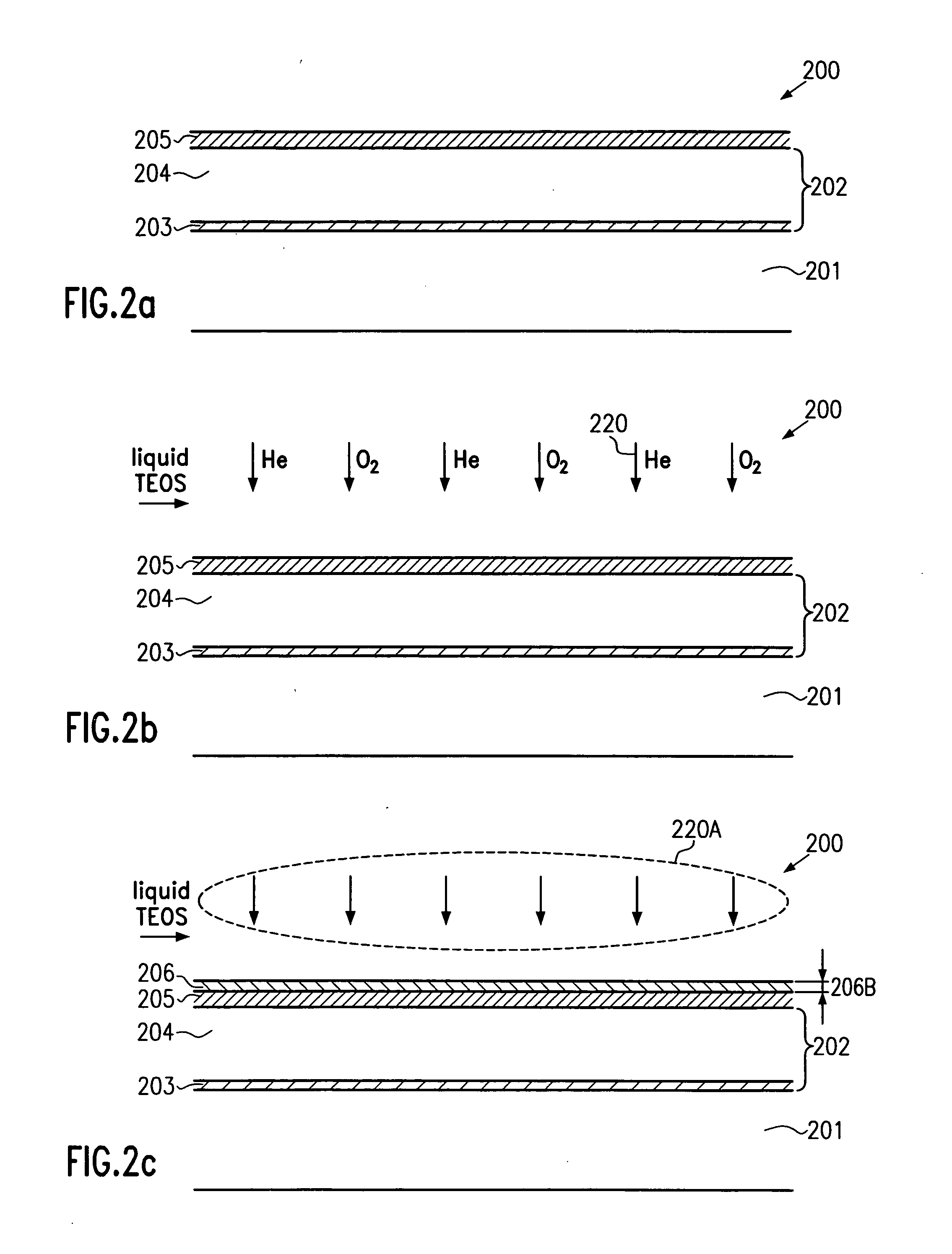
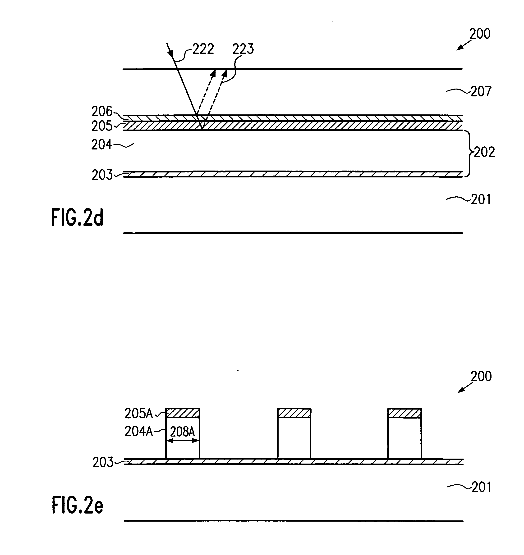
[0017] Generally, the present invention is directed to a method for forming a silicon dioxide cap layer on an amorphous carbon hard mask layer for patterning a polysilicon feature. Without restricting the present invention to the following explanation, it is believed that the provision of a silicon dioxide layer formed by plasma enhanced chemical vapor deposition at temperatures of 370° C. and less may significantly reduce the defectiveness of the finally obtained polysilicon features. Based on this finding, the plasma enhanced CVD process for forming a silicon dioxide layer is designed so as to enable reliable control of a thickness of the silicon dioxide layer within a range of 5-50 nm, as is required for providing the desired optical characteristics in combination with the underlying amorphous carbon layer. Since, typically, a TEOS-based plasma enhanced CVD process exhibits an enhanced deposition rate at lower temperatures, which, according to the present invention, are required to reduce the defect rate, in some embodiments, the deposition process is controlled to provide a reduced deposition rate so as to enable a reliable control of the layer thickness, thereby assuring the required optical characteristics of the silicon dioxide / amorphous carbon layer stack.

Problems solved by technology

Thus, merely reducing the wavelength of light sources for lithography apparatus is not a straightforward development and may not easily be implemented in mass production of circuit elements having feature sizes of 50 nm and less.
Since the continuous device scaling requires extending the concept of resist trimming even further to obtain the desired reduced critical dimension for a given exposure wavelength, the resist layer thickness has to be adapted to the increased resist material removal during the trim process, thereby significantly deteriorating the optical characteristics of the layer stack comprised of the resist and the bottom anti-reflective coating (ARC).
Particularly the reflectivity of the bottom ARC significantly affects the line width after the lithography and causes variations thereof that may not be efficiently compensated for by the subsequent trim process within the tight process tolerances dictated by the design rules.
As previously discussed, the reflectivity of an anti-reflective coating during the patterning of a polysilicon layer may significantly affect the accuracy of the resist trim process, thereby also influencing the finally-obtained gate length of the polysilicon feature.
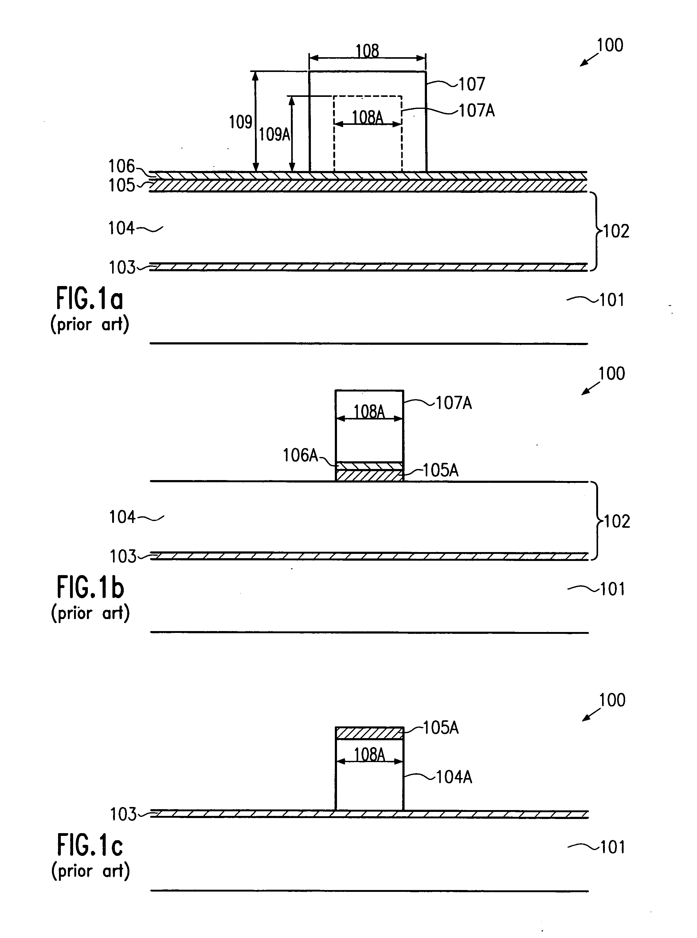
The reason for this may be chemical reaction between the carbon and the photoresist at the interface thereof, thereby possibly altering the optical characteristics of the photoresist and causing insufficiently developed resist portions that may then be patterned into the polysilicon line 104.
For instance, a cap layer 106 comprised of silicon oyxnitride exhibits a significant defect rate, thereby rendering the formation process unreliable, while the provision of a cap layer 106 in the form of a silicon dioxide may have the potential to reduce the defect rate, wherein a corresponding conventional deposition process may not be controlled in a reliable manner according to presently available process recipes.

Method used


Image

  • Method of forming a teos cap layer at low temperature and reduced deposition rate
  • Method of forming a teos cap layer at low temperature and reduced deposition rate
  • Method of forming a teos cap layer at low temperature and reduced deposition rate

Examples


Embodiment Construction

[0024] Illustrative embodiments of the invention are described below. In the interest of clarity, not all features of an actual implementation are described in this specification. It will of course be appreciated that in the development of any such actual embodiment, numerous implementation-specific decisions must be made to achieve the developers' specific goals, such as compliance with system-related and business-related constraints, which will vary from one implementation to another. Moreover, it will be appreciated that such a development effort might be complex and time-consuming, but would nevertheless be a routine undertaking for those of ordinary skill in the art having the benefit of this disclosure.

[0025] The present invention will now be described with reference to the attached figures. Although the various regions and structures of a semiconductor device are depicted in the drawings as having very precise, sharp configurations and profiles, those skilled in the art reco...


PUM

PropertyMeasurementUnit
thicknessaaaaaaaaaa
temperatureaaaaaaaaaa

Abstract

The present invention discloses a method for forming a silicon dioxide cap layer for a carbon hard mask layer for patterning of polysilicon line features having critical dimensions of 50 nm and less. To this end, a low temperature plasma enhanced CVD process is used in which the deposition rate is maintained low to provide improved controllability of the layer thickness and, thus, of the optical characteristics of the silicon dioxide layer.

Description

BACKGROUND OF THE INVENTION [0001] 1. Field of the Invention [0002] The present invention generally relates to the fabrication of integrated circuits, and, more particularly, to the formation of small circuit elements, such as a gate electrode of a field effect transistor, on a substrate by sophisticated trim etch techniques requiring advanced masking schemes, wherein the dimensions of the circuit elements are significantly less than the resolution of the involved lithography technique. [0003] 2. Description of the Related Art [0004] The trend in recent years to steadily decrease the feature sizes of circuit elements in integrated circuits will continue in the near future, wherein reproducible and robust processes have to be established that allow the formation of a huge number of integrated circuits in a cost-efficient manner. Presently, sophisticated integrated circuits that are available as mass products include elements having dimensions which are well below the optical resoluti...

Claims


Application Information

Patent Timeline
Patent Type & Authority Applications(United States)
IPC IPC(8): C23C16/40H01L21/027H01L21/033H01L21/314H01L21/316H01L21/3213
CPCC23C16/402H01L21/02164H01L21/02274H01L21/0276H01L21/32139H01L21/3146H01L21/31612H01L21/32137H01L21/0332H01L21/02126
Inventor RUELKE, HARTMUTHUY, KATJAROMERO, KARLA
Owner GLOBALFOUNDRIES INC
Learn More