Method for patterning organic materials or combinations of organic and inorganic materials

Inactive Publication Date: 2005-03-03
SONY DEUT GMBH
View PDF7 Cites 61 Cited by
  • Summary
  • Abstract
  • Description
  • Claims
  • Application Information

AI Technical Summary

Problems solved by technology

However, for patterning of organic materials, photoresists have the disadvantage that they also rely on organic solvents.
However, organic materials are not stable at such temperature and the possibility of using the water soluble CaO mask to pattern organic or organic/inorganic materials was not attempted or described.
The major shortcoming of this technique is the low speed due to serial writing (non-parallel processing).
One of the disadvantages of this approach is that the etching solution for aluminium has to have either relatively high or low pH values.
Such conditions are not compatible with many material systems.
In addition, oxygen plasma etching of inorganic/organic composites may lead to residual inorganic material on the wafer surface.
Further disadvantages are: (a) the whole substrate has first to be unselectively coated with the nanoparticle component; (b) harsh etching conditions have to be applied to remove the particles on non-covered parts; (c) this destructive technique may not be compatible with circuit elements on the chip as well as other materials, which are already deposited on the substrate.
The resolution is limited by the accuracy of the stamp.
Also, this meth

Method used


Image

  • Method for patterning organic materials or combinations of organic and inorganic materials
  • Method for patterning organic materials or combinations of organic and inorganic materials
  • Method for patterning organic materials or combinations of organic and inorganic materials

Examples


example 1

Patterning Organic or Organic / Inorganic Materials—Route A

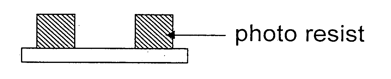
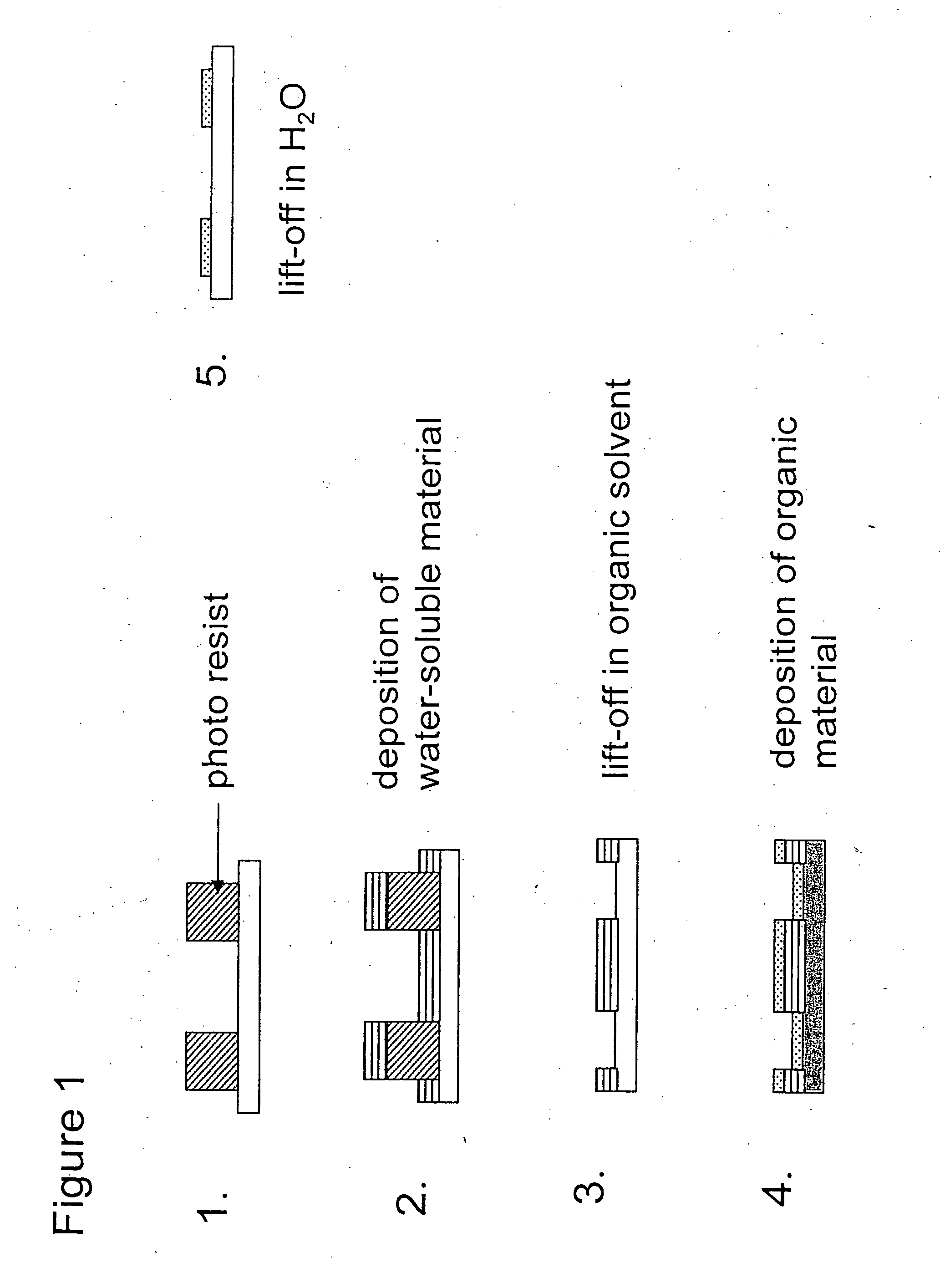
[0123] Step 1: A photoresist mask is patterned by either photolithography, electron beam lithography, or printing onto a solid or soft substrate (see Step 1 of FIG. 1.)

[0124] The thickness of the mask material “A” can be varied in large range between less than 1 nm and more than 2 μm. Preferably, the mask thickness should be larger than the thickness of the deposited material “B” (see below) in order to provide a successful lift-off.

[0125] In addition, it can be advantageous to cover the water-soluble mask by a thin layer of insoluble material like aluminium, ZrO2, or other materials that can form thin layers. This would stabilise the water-soluble mask during the process steps (against humidity, for example).

[0126] Step 2: 1 to 20,000 nm (preferably 20 to 1,000 nm) of water-soluble materials (material “A”) is deposited by thermal evaporation (including e-gun) or sputtering, or is spin-coated onto this photomask (see Step,...

example 2

Patterning Organic or Organic / Inorganic Materials—Route B

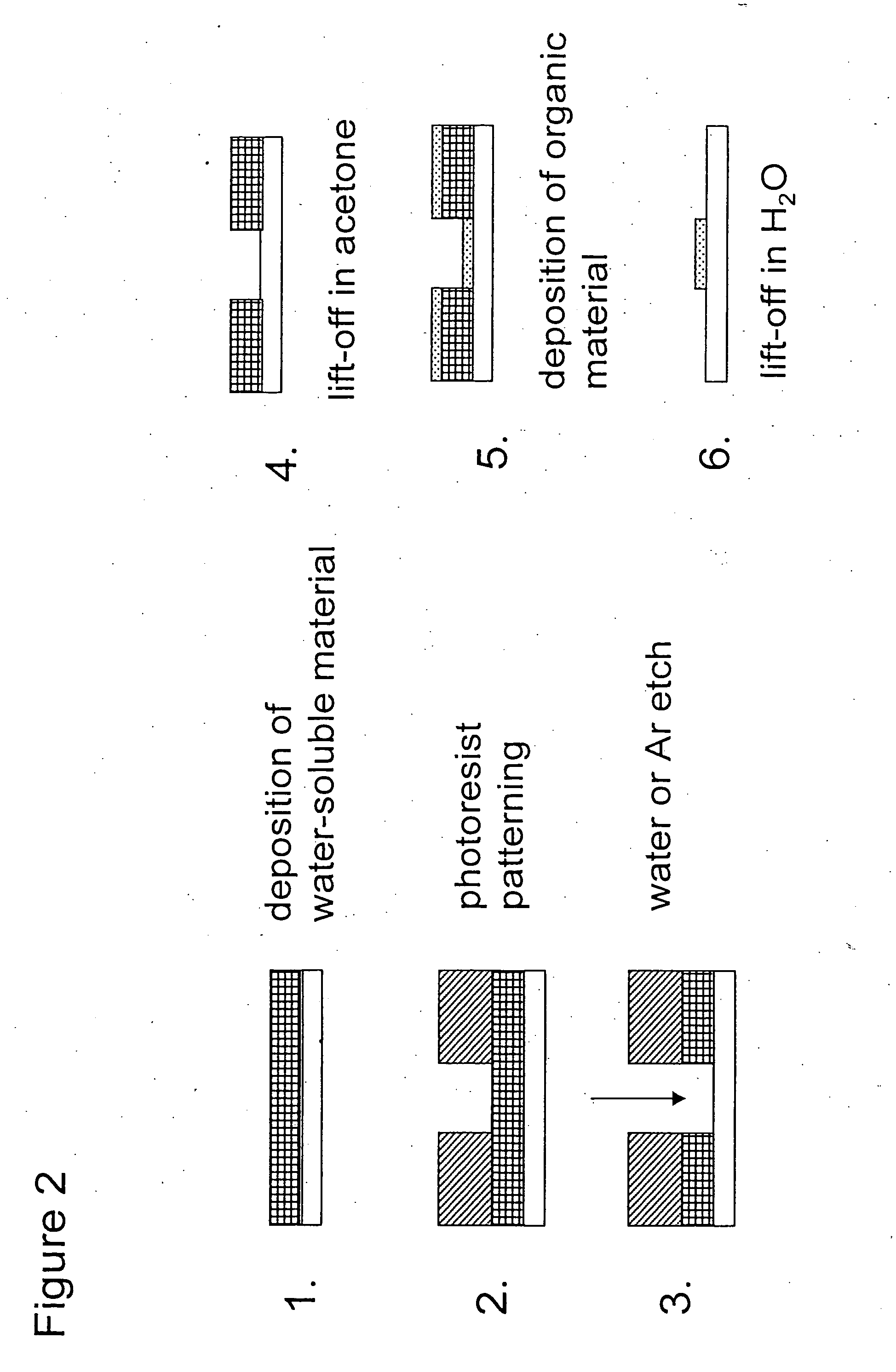
[0132] The above described process steps of Route “A” can also be arranged in a slightly different order. In this case, the water-soluble material “A” is deposited on a solid or soft substrate first and then, structures are introduced through a lithographic step on top of the water-soluble mask and subsequent water-etching.

[0133] Step 1: Typically 100 to 200 nm of water-soluble material (material “A”) is deposited by thermal evaporation (including e-gun), or sputtering, or is spin-coated onto a solid or soft substrate (see Step 1 of FIG. 2). The deposition rate can be in the range of less than 1 Å / s up to more than 100 nm / s. In the case that metallic material is deposited which has to be changed into a water-soluble oxide, the chamber can be partly (sputtering) or completely filled (preferably after deposition) with oxygen, oxygen plasma or ambient atmosphere. Material “A” can be any kind of water-soluble material from the g...

example 3a

Patterning of an Inorganic / Organic Composite Film Comprised of Gold Nanoparticles and Organic Linker Molecules (Route A)

[0143] In this example, it is demonstrated that a layer of Ca / CaO / Ca(OH)2 can be employed as water-soluble mask material “A” to pattern a composite film from gold nanoparticles and organic linker molecules.

[0144] Step 1: Standard Ti35zE or Az5214 photoresist was spin-coated onto a silicon wafer or glass wafer at 4,000 rpm to a final thickness of about 3 μm. After baking at 90° C. for 2 minutes, the resist was exposed for 10 seconds at 365 nm using a contact aligner. Then, the resist was developed in MIF826 developer for 1 to 2 minutes and rinsed with water.

[0145] Alternatively, UV6.06 electron beam resist was spin-coated at 4,000 rpm and baked at 130° C. for 60 seconds. Then the resist was exposed at 10 kV using a dose of about 15 μC / cm2. FIG. 3 shows an optical microscope picture of the electron beam resist structure after development.

[0146] Step 2: 25 to 200 ...


PUM


Abstract

The present application refers to a method of patterning organic materials or organic/inorganic materials onto a substrate, comprising the following steps: (1) patterning of a water-soluble material “A” onto a surface of the substrate, thereby forming a substrate/material “A” surface; (2) depositing organic or organic/inorganic material “B” onto the substrate/material “A” surface; (3) lifting-off material “A” in aqueous solution; wherein, step (1) comprises the following steps: (1a) patterning of a photoresist material onto the substrate surface, thereby forming a substrate/photoresist material surface; (1b) depositing the water soluble material “A” onto the substrate/photoresist material surface; (1c) lifting-off the photoresist material in an organic solvent; or, alternatively, step (1) comprises the following steps: (1a′) depositing the water-soluble material “A” onto the substrate surface, thereby forming a substrate/material “A” surface; (1b′) patterning the photoresist material onto the substrate/material “A” surface; (1c′) etching the unmasked material “A” in aqueous solution; (1d′) lifting-off the photoresist material in an organic solvent. The present application also refers to the use of said method, to a pattern of organic materials or organic/inorganic materials prepared by said method, and to a substrate carrying such patterns. The application also refers to the use of a patterned nanoparticle film.

Description

[0001] The present application refers to a method of patterning organic materials or organic / inorganic materials onto a substrate, and also refers to the use of said method. The application further refers to a pattern of organic or organic / inorganic materials prepared by the method of the present application, and to a substrate carrying such patterns. The application also refers to the use of a patterned nanoparticle film. BACKGROUND OF THE INVENTION [0002] A basic requirement for developing organic devices and devices based on organic / inorganic composite materials is the presence of a patterning technology which is solvent-compatible with organic materials. Various photoresist systems are widely used for patterning inorganic materials. However, for patterning of organic materials, photoresists have the disadvantage that they also rely on organic solvents. If the solvent of the photoresist system comes into contact with the organic material then mixing and lifting of the organic mat...

Claims


Application Information

Patent Timeline
IPC IPC(8): H05B33/10G03F7/00H01L21/28H01L21/306H01L21/3205H01L29/06H01L51/50H05K3/02H05K3/04
CPCB82Y30/00H05K3/048G03F7/0035G03F7/00B82B3/00B82Y40/00
Inventor HARNACK, OLIVERRAIBLE, ISABELLEYASUDA, AKIOVOSSMEYER, TOBIAS
Owner SONY DEUT GMBH
Why Eureka
Try Eureka