Plasma processing apparatus

a processing apparatus and plasma technology, applied in the direction of electrolysis process, electrolysis components, electric discharge tubes, etc., can solve the problems of deterioration of selectivity with respect to resist or substrate, plasma density and ion energy incident on the wafer cannot be controlled independently, and achieve high uniformity, high accuracy, and high accuracy processing stably

Inactive Publication Date: 2005-03-10
HITACHI HIGH-TECH CORP
View PDF7 Cites 42 Cited by
  • Summary
  • Abstract
  • Description
  • Claims
  • Application Information

AI Technical Summary

Benefits of technology

[0018] The object of the present invention is to provide a plasma processing apparatus capable of processing a wafer having a diameter of 300 mm or larger with high uniformity and high accuracy. Another object of the

Problems solved by technology

However, the RIE device has a drawback in that the plasma density and the ion energy incident on the wafer cannot be controlled independently, since the source power for generating the plasma and the bias power for drawing ions toward the wafer are common.
CF-based gases are mainly used to etch silicon oxide films, but multiple dissociation of the CF-based gas is caused by plasma, which inevitably generates F radicals causing deterioration of the selectivity with respect to the resist or the substrate nitride film.
It is extremely unfavorable from the point of view of stability and contamination for the plasma to spread to regions other than directly above the processed wafer, that is, approximate the side walls or the bottom wall of the reaction chamber or under the electrode.
The damaging of side walls or other parts of the reaction container by the plasma spreading to regions other than directly above the wafer causes heavy-metal contamination of the wafer or generation of particles, leading to significant deterioration of the yield factor.
If a gas having a strong deposition property is used, deposition is formed to the side walls of the container, causing contaminants to be produced when the deposition on the side walls fall off.
However, it is difficult for such prior art apparatus to correspond to a next-generation processing in which the object is further shrinked.
That is, processing under lower pressure is desirable to cope with microfabrication, but it is known that when 27.12 MHz frequency is applied as source power, it is difficult to generate plasma with a sufficient density to realize processing under a pressure as low as around 0.2 Pa to 4 Pa.
Applying greater source power to increase the plasma density is not desirable, not only because it deteriorates efficiency, but also because it increases the density of unnecessary plasma diffusing from above the wafer.
Furthermore, the shield ring and the baffle plate that contribute to preventing the unnecessary diffusion of plasma and improving the efficiency of the source power in the prior art apparatus can not exert these effects sufficiently under a low pressure condition in which the diffusion velocity of plasma is high.
Another drawback of the prior art apparatus is that when the shield ring and baffle plate are

Method used


Image

  • Plasma processing apparatus
  • Plasma processing apparatus
  • Plasma processing apparatus

Examples


second embodiment

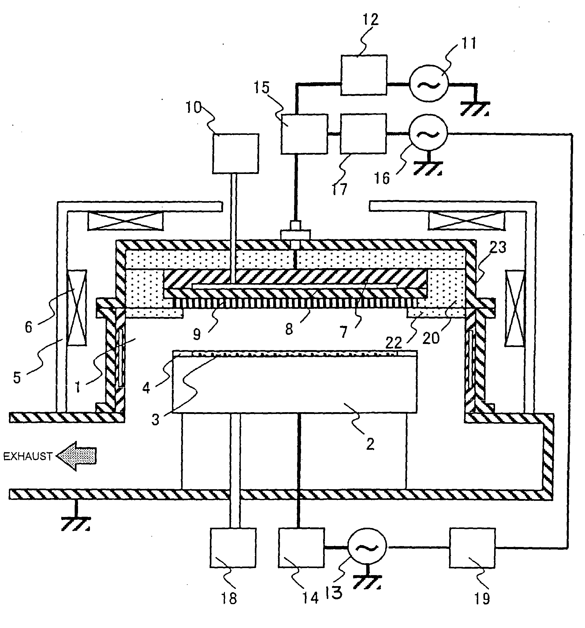
[0073] the invention comprises, in addition to the yoke 5 and coil 6 being the first means for generating a magnetic field in the discharge space, a substantially ring-shaped second magnetic field forming means 21 disposed above the antenna. The second magnetic field forming means 21 is a permanent magnet made of materials such as ferrite, samarium-cobalt or neodymium-ferrum-boron, the use of which allows a more detailed magnetic field control inside the discharge space at low cost.

first embodiment

[0074] In the first embodiment, the magnetic field forming means comprises only a yoke 5 and a coil 6, and in order to carry out fine magnetic field control, two lines of coils to which are supplied different currents from separate DC power sources are disposed so as to control the magnetic field intensity and the shape of the lines of magnetic force. If there is only one line of coil 6, only the magnetic field intensity can be controlled and thus the control range is narrowed. On the other hand, if the number of coils and the number of DC power sources connected thereto are increased, the manufacturing cost and running cost of the apparatus are increased, and thus the cost of the semiconductor device manufactured using the plasma processing apparatus is increased.

[0075] According to the second embodiment introducing the second magnetic field generator 21, both the magnetic field intensity and the shape of the line of magnetic force can be varied simultaneously using only one coil a...

third embodiment

[0082] The third embodiment does not comprise a third high frequency power source for actually controlling the active species in the gas or a third impedance matching network. Though the controllability of the active species in the gas is somewhat deteriorated, the manufacturing and running costs of the apparatus are cut down. Moreover, though not shown in FIG. 9, it is possible to provide two series of process gas supplying to the apparatus so as to control the density and distribution of active species within the gas.

[0083] As explained above, the third embodiment of the present invention provides a plasma processing apparatus that can be manufactured and operated at lower cost.


PUM

PropertyMeasurementUnit
Lengthaaaaaaaaaa
Diameteraaaaaaaaaa
Frequencyaaaaaaaaaa

Abstract

A plasma processing apparatus capable of processing a wafer having a diameter of 300 mm or greater with high accuracy and uniformity, the apparatus comprising a decompressable container 1, a stage 2 disposed within container 1 and supporting a wafer 3 thereon, a substantially circular conductive plate 7 disposed substantially in parallel with the wafer 3 and opposing the stage 2, and a high frequency power source 11 connected to the conductive plate 7 and supplying power to generate a plasma within a space interposed between the stage 2 and the conductive plate 7, characterized in that a frequency f1 of the power is within the range of 100 MHz<F1<(0.6×C)/(2.0×D) Hz with respect to a speed of light C in vacuum and a diameter D of the wafer being processed.

Description

FIELD OF THE INVENTION [0001] The present invention relates to a plasma processing apparatus that utilizes a plasma generated within a decompressed chamber to carry out processes such as etching and ashing to a substrate such as a semiconductor wafer. DESCRIPTION OF THE RELATED ART [0002] In the field of semiconductor device fabrication, plasma processing apparatuses are widely used for deposition and etching processes. Along with the shrinking of the device or the enlarging of the wafer diameter, there are increasing demands for higher performance of the plasma processing apparatus. Taking a plasma etching apparatus as an example, there are demands for higher processing performances such as vertical workability (anisotropic etching), higher selectivity and workability with respect to the mask material or substrate material, higher etching rate and uniform processing, and for techniques to maintain the processing performance for a long period of time. [0003] There have been various ...

Claims


Application Information

Patent Timeline
IPC IPC(8): C25B9/00H01J37/32H01L21/306H01L21/311
CPCH01L21/31116H01J37/32082
Inventor MAEDA, KENJIYOKOGAWA, KENETSUYOSHIDA, TSUYOSHI
Owner HITACHI HIGH-TECH CORP
Why Eureka
Try Eureka