Magnetic memory device and method of manufacturing the same

Inactive Publication Date: 2005-03-10
SONY CORP
View PDF6 Cites 24 Cited by
  • Summary
  • Abstract
  • Description
  • Claims
  • Application Information

AI Technical Summary

Benefits of technology

[0075] In the present invention, at least the soft magnetic material layer constituting the cladding structure of the first wiring (word line) and/or the second wiring (bit line) is formed by electroless plating, and therefore the soft magnetic material layer can be formed around the main wiring material (especially copper) in the first and/or second wiring so that the soft magnetic material layer has a uniform, satisfactory thickness. Thus, an induced magnetic field generated at the first and/or second wiring can be efficiently introduced to the memory element, and hence the current fed to the wiring required for generating the magnetic field can be reduced, so that not only can the power consumption of the magnetic storage device be lowered, but also the storage sensitivity can be improved. Therefore, there is no need to reduce the distance between each wiring and the memory element for improving the write efficiency of the first and/or second wiring, making it possible to expand the process margin in formation of the insulating layer therebetween.
[0076] In this case, a material having magnetic properties, such as nickel or an alloy thereof, or cobalt or an alloy thereof, can be easily deposited by electroless plating, and, when depositing an alloy film or the like, the composition of the film can be easily changed by controlling the plating solution or plating conditions, thus making it possible to easily obtain the required soft magnetic material properties.
[0077] The at least soft magnetic material layer is formed by electroless plating, and therefore it can be deposited with improved uniformity on the surface with which the electroless plating solution is in contact, and the uniformity of cladding is improved at not only the bottom surface but also the sidewall of a wiring trench, so that the soft magnetic material layer formed has a required minimum volume or thickness, making it possible to render the volume of the main wiring material (especially copper) relatively large. Therefore, the resistance of the wiring is reduced and the effective current density is further lowered, thus improving the wiring reli

Problems solved by technology

However, in accordance with the current design rule scaled-down, a problem of unsatisfactory cladding in the sputtering surfaces.
However, in the quarter of micron size or less, the conven

Method used


Image

  • Magnetic memory device and method of manufacturing the same
  • Magnetic memory device and method of manufacturing the same
  • Magnetic memory device and method of manufacturing the same

Examples


Example

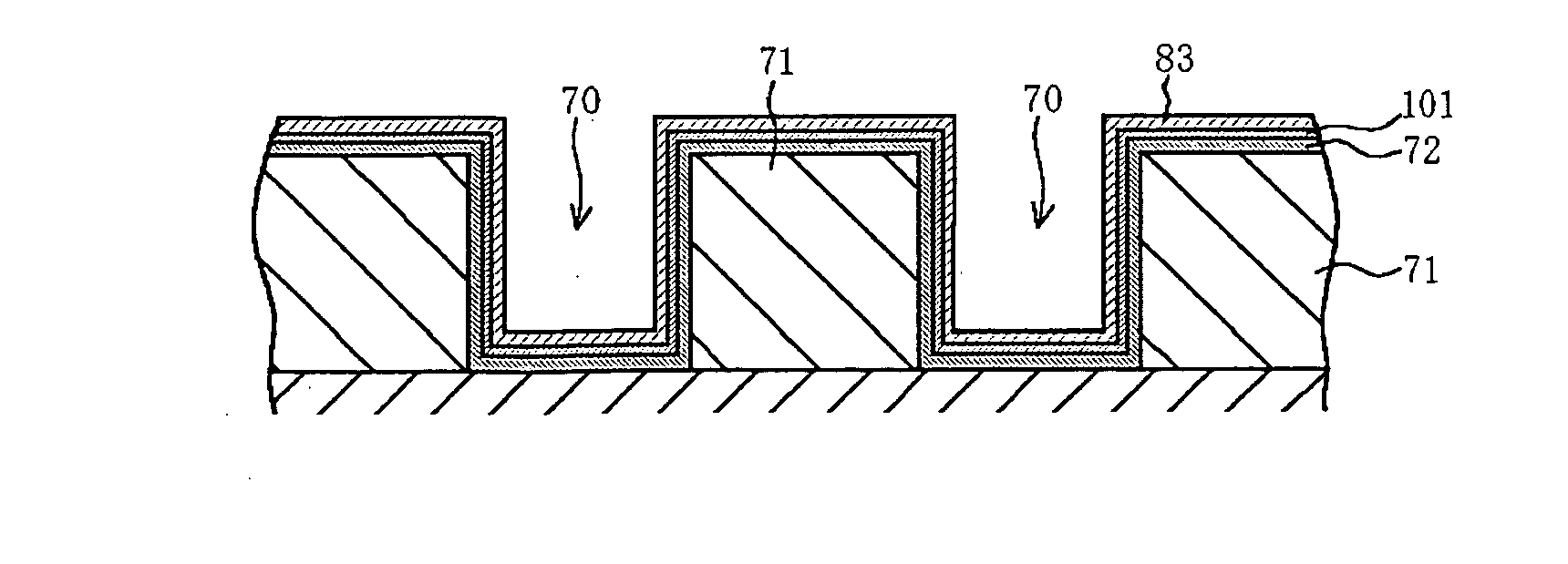
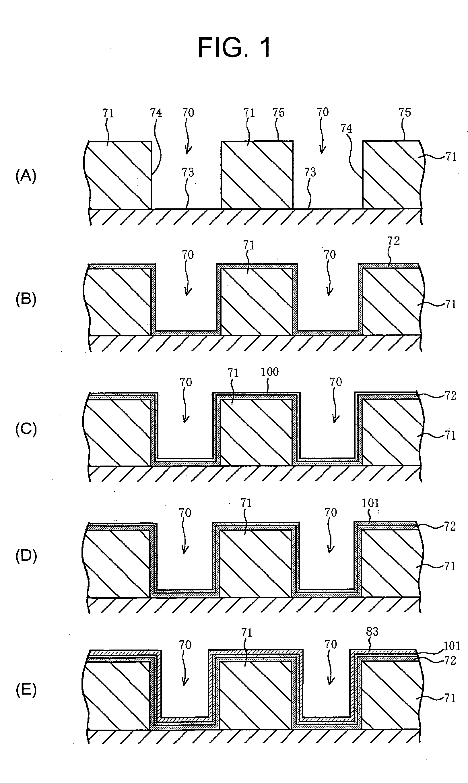
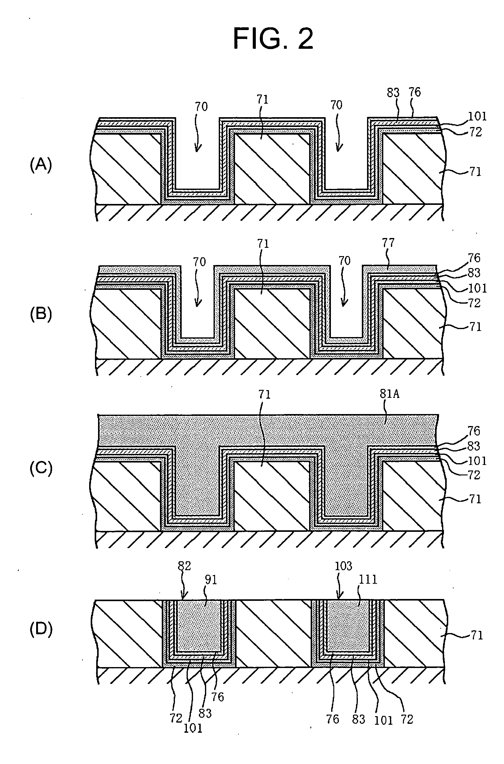
[0110] In the magnetic storage device according to a preferred embodiment of the present invention and the method of manufacturing the same, when the soft magnetic material layer and a diffusion barrier layer are formed in the trench at each outer periphery portion of the first wiring and the second wiring wherein the buried conductor (especially copper or a copper alloy) of the first wiring and / or the second wiring, the soft magnetic material layer, and the diffusion barrier layer are individually formed by electroless plating, the above-mentioned effect of the present invention is further improved.

[0111] It is desired that the first wiring and the second wiring are formed from copper or a copper alloy.

[0112] It is desired that the present invention is applied to a magnetic random access memory constituted so that a storage layer of the memory element is magnetized in a predetermined direction by means of a magnetic field induced by allowing a current to flow individually the fir...


PUM


Abstract

A magnetic memory device and a method of manufacturing the same, which are advantageous not only in that both the improvement of storage sensitivity and the reduction of power consumption can be achieved, but also in that a buried wiring having low resistance and high reliability can be formed in reduced time in a stable manner. Soft magnetic material layers forming the cladding structure of a word line and a bit line constituting an MRAM are formed by electroless plating, and the soft magnetic material layers are formed around main wirings (especially copper) of the word line and bit line so that the soft magnetic material layers individually have a uniform, satisfactory thickness, and further they are deposited with improved uniformity on the surface with which the electroless plating solution is in contact, and therefore the uniformity of cladding is improved at not only the bottom surface but also the sidewall of a wiring trench.

Description

CROSS REFERENCE TO RELATED APPLICATIONS [0001] The present document is based on Japanese Priority Application JP2003-297593 filed to the Japanese Patent Office on Aug. 21, 2003, the content of which being incorporated herein by reference to the extent permitted by law. BACKGROUND OF THE INVENTION [0002] 1. Field of the Invention [0003] The present invention relates to a magnetic storage device and a method of manufacturing the same. More particularly, it relates to a nonvolatile magnetic storage device which stores information by utilizing a change in resistance caused by changing of the direction of spin of a ferromagnetic material to parallel or non-parallel, and a method of manufacturing the magnetic storage device. [0004] 2. Related Art [0005] As information communication machines and apparatuses, especially personal compact apparatuses, such as portable terminals become increasingly popular, there are demands for devices of higher performance, such as memory elements and logic ...

Claims


Application Information

Patent Timeline
IPC IPC(8): G11C11/15H01L27/105G11C11/16H01L21/8246H01L27/22H01L43/08
CPCB82Y10/00H01L43/12H01L27/228G11C11/16H10B61/00H10B61/22H10N50/01G11C11/15
Inventor HORIKOSHI, HIROSHI
Owner SONY CORP
Why Eureka
Try Eureka