Nitride semiconductor device and manufacturing method thereof

Inactive Publication Date: 2005-03-10
NICHIA CORP
View PDF11 Cites 12 Cited by
  • Summary
  • Abstract
  • Description
  • Claims
  • Application Information

AI Technical Summary

Benefits of technology

[0026] On the other hand, when the GaN substrate comprising a heterogeneous substrate and nitride semiconductor layers is used, the breakage and chipping of the wafer can be prevented, with the result that good handling properties can be achieved. Moreover, the step of removing the auxiliary substrate can be eliminated and the manufacturing time is shortened. Even when the GaN substrate comprises a heterogeneous substrate, if the substrate is electrically conductive, the n-electrode can

Problems solved by technology

However, in some applications, much longer lifetime is desired.
The inventors examined the nitride semiconductor laser device obtained by the above-described method and found that extremely small cracks tend to occur in the nitride semiconductor layers grown on the GaN substrate, particularly in the n-type GaN contact layer which is grown directly on the GaN substrate.
The crack is too small to observe by a typical optical microscope, however, it can be observed by a fluorescence microscope.
It is a surprising

Method used


Image

  • Nitride semiconductor device and manufacturing method thereof
  • Nitride semiconductor device and manufacturing method thereof
  • Nitride semiconductor device and manufacturing method thereof

Examples


example 1

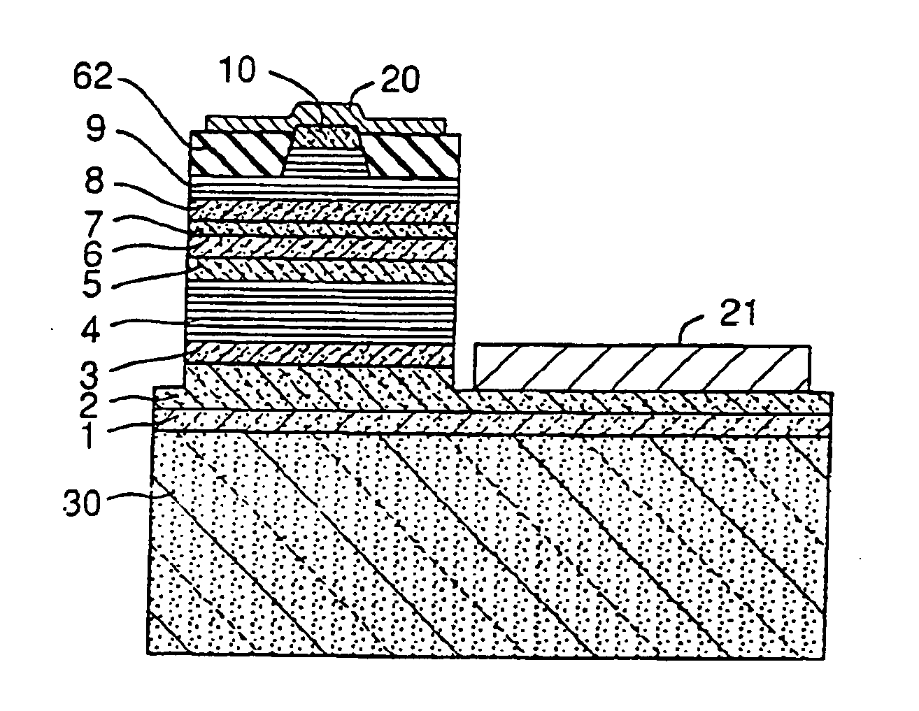
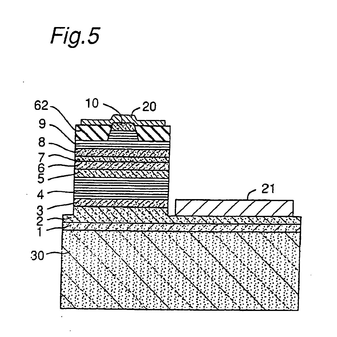
[0051] In Example 1, the nitride semiconductor laser device as shown in FIG. 5 was manufactured.

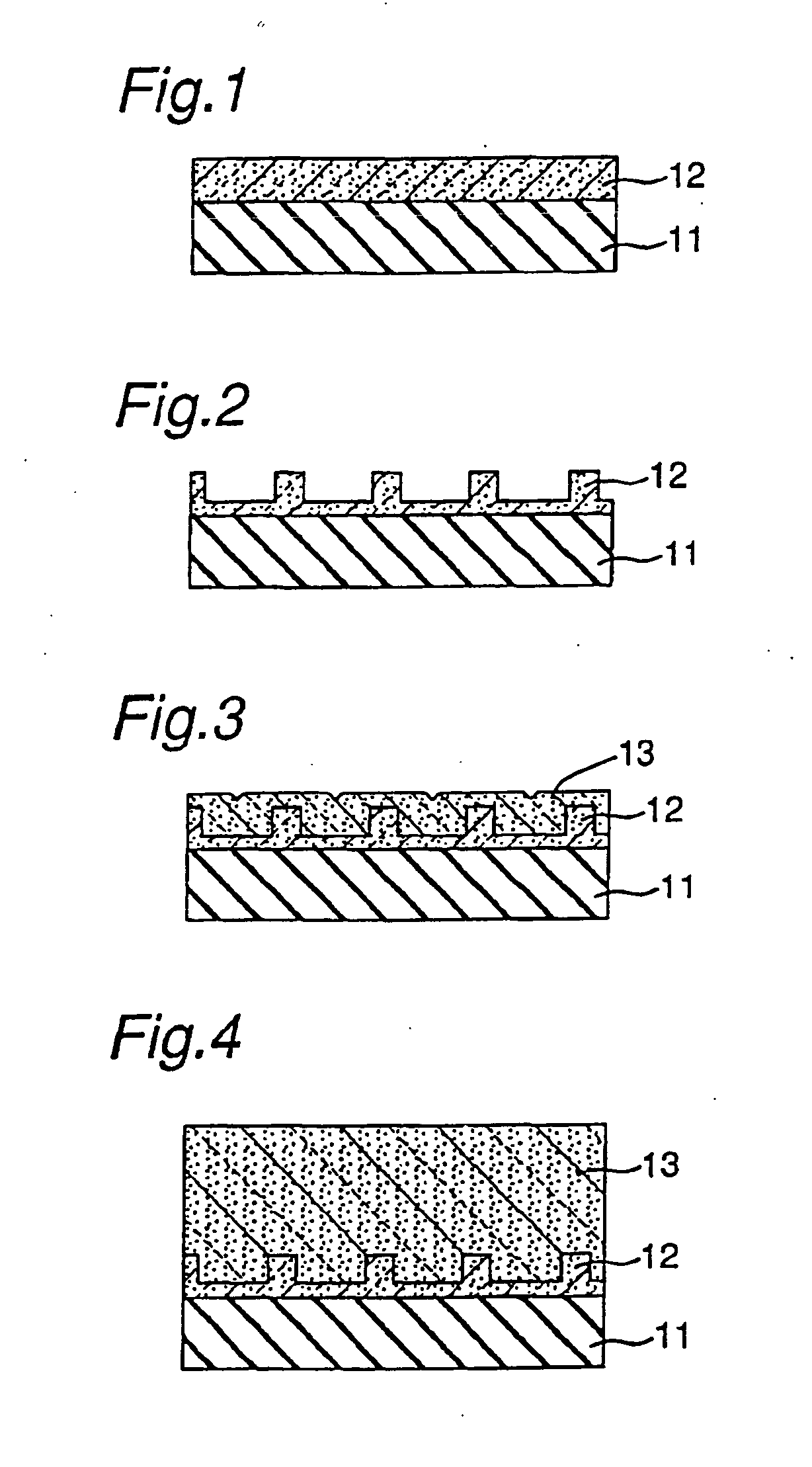
[0052] (Manufacturing Method of the GaN Substrate)

[0053] The GaN substrate was manufactured according to each step as shown in FIGS. 1 to 4.

[0054] A sapphire substrate 11 of two-inch in diameter having its principal surface represented by a C-face and an orientation flat face represented by an A-face was set in the reactor and the temperature was adjusted to 510° C. A buffer layer (not shown) made of GaN which has a thickness of about 200 angstroms was grown using hydrogen as a carrier gas and ammonia and TMG (trimethylgallium) as a source of GaN on the sapphire substrate.

[0055] After growing the buffer layer, only TMG was stopped and the temperature was increased to 1050° C. At 1050° C., using ammonia and TMG as a source of GaN, a first nitride semiconductor layer 12 made of undoped GaN was grown to the thickness of 2 μm (FIG. 1).

[0056] After growing a first nitride semiconductor la...

example 2

[0093] The laser device was fabricated in the same manner as in Example 1, except that the undoped n-type contact layer 1 was not grown and only the n-type contact layer 2 was grown.

[0094] The resulting device had a crystallinity which was a little worse than that in Example 1. But small cracks could be prevented almost like in Example 1 and good device characteristics could be achieved.

example 3

[0095] The laser device was fabricated in the same manner as in Example 1, except that the ratio of Al in the undoped n-type contact layer 1 and the Si-doped n-type contact layer 2 was changed from 0.05 to 0.2.

[0096] The resulting device showed good result almost like in Example 1.


PUM


Abstract

A nitride semiconductor device includes a GaN substrate having a single-crystal GaN layer at least on its surface and plurality of device-forming layers made of nitride semiconductor. The device-forming layer contacting the GaN substrate has a coefficient of thermal expansion smaller than that of GaN, so that a compressive strain is applied to the device-forming layer. This result in prevention of crack forming in the device-forming layers, and a lifetime characteristics of the nitride semiconductor device is improved.

Description

TECHNICAL FIELD OF THE INVENTION [0001] This invention relates to a device provided with a nitride semiconductor (InxAlyGa1-x-yN, 0≦x, 0≦y, x+y≦1) including light emitting diode (LED), laser diode (LD), or other electronic devices and power devices. Particularly, the present invention relates to a prevention of a small cracking in nitride semiconductor layers, which occurs in the nitride semiconductor device using a GaN substrate. BACKGROUND OF THE INVENTION [0002] Blue LEDs using nitride semiconductors have already been provided for practical use. Recently, it becomes possible to provide a practical blue laser diode made of nitride semiconductor by using a GaN substrate. [0003] The inventors have disclosed a nitride semiconductor laser diode using a GaN substrate in, for example, Japanese Journal of Applied Physics. Vol.37(1998) pp.L309-L312. The GaN substrate can be formed, for example, by the following method: A GaN layer is formed on a sapphire substrate and a protective film ma...

Claims


Application Information

Patent Timeline
IPC IPC(8): H01L21/20H01L21/205H01L33/00H01L33/06H01L33/12H01L33/14H01L33/22H01L33/32H01S5/02H01S5/32H01S5/323H01S5/343
CPCC30B25/20H01S2301/173H01L21/02378H01L21/0242H01L21/0243H01L21/02458H01L21/0254H01L21/0262H01L21/02639H01L33/0075H01S5/021H01S5/0422H01S5/3201H01S5/32341C30B29/403H01S5/0421H01S2304/04
Inventor NAGAHAMA, SHINICHINAKAMURA, SHUJI
Owner NICHIA CORP
Why Eureka
Try Eureka