Semiconductor device and a method of manufacturing the same

a semiconductor device and semiconductor technology, applied in the field of semiconductor devices, can solve the problems of difficult to reduce the size of memory cells, and achieve the effect of improving the characteristics of semiconductor devices

Inactive Publication Date: 2005-03-17
RENESAS TECH CORP
View PDF1 Cites 97 Cited by
  • Summary
  • Abstract
  • Description
  • Claims
  • Application Information

AI Technical Summary

Benefits of technology

Advantageous effects obtained by typical features of the invention among those described in the present application will be explained simply below.
The characteristics of the semiconductor device can be improved.
In the following description, while the subject matter will be described while being divided into plural sections or embodiments, when necessary for the sake of convenience; however, they are not irrelevant to each other, but are in such a relation that one constitutes a modified example, details or a complementary description of a portion or the entirety of the others. Further, when a number of elements (including, for example, number, numerical value, quantity, range, etc.) is referred to in the following description of the embodiments, they are not restricted to any particular number, but may be more than or less than the particular number, unless otherwise described clearly or apparently restricted to a particular number in principle. Furthermore, in the following description of the embodiments, it will be apparent that the constituent elements (also including elemental steps, etc.) are not always essential, unless otherwise described specifically or considered apparently essential in principle. In the same manner, when the configuration, position, relation, etc. is referred to in the following description of the embodiments, they include those substantially approximate or similar to the shape, etc., unless otherwise described specifically or considered apparently not so in principle. This is also applicable to the numerical value and the range mentioned above. Further, in the drawings, even a plan view may sometimes be hatched for easy understanding of features of the drawings. Further, throughout the drawings, identical components are identified by the same reference numerals and duplicate descriptions thereof will be omitted.

Problems solved by technology

However, in the so-called complete CMOS (Complementary-Metal-Oxide-Semiconductor) type SRAM of this type, since six MISFETs are arranged in a planar manner on the main surface of a semiconductor substrate, it is difficult to reduce the size of the memory cell.
That is, in the complete CMOS type SRAM requiring p- and n-type well regions for forming the CMOS and a well isolation region for isolation between a n-channel type MISFET and a p-channel type MISFET, it is difficult to reduce the size of the memory cell.

Method used


Image

  • Semiconductor device and a method of manufacturing the same
  • Semiconductor device and a method of manufacturing the same
  • Semiconductor device and a method of manufacturing the same

Examples


embodiment 1

(Embodiment 1)

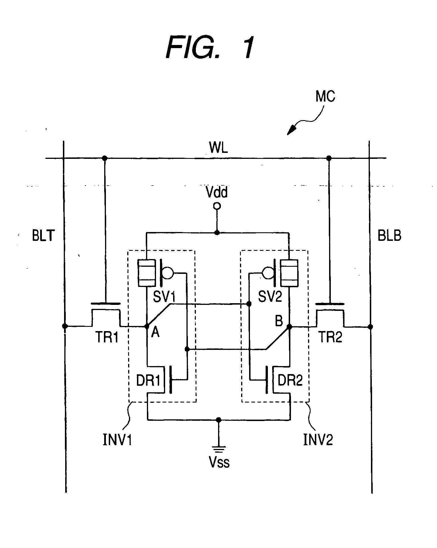
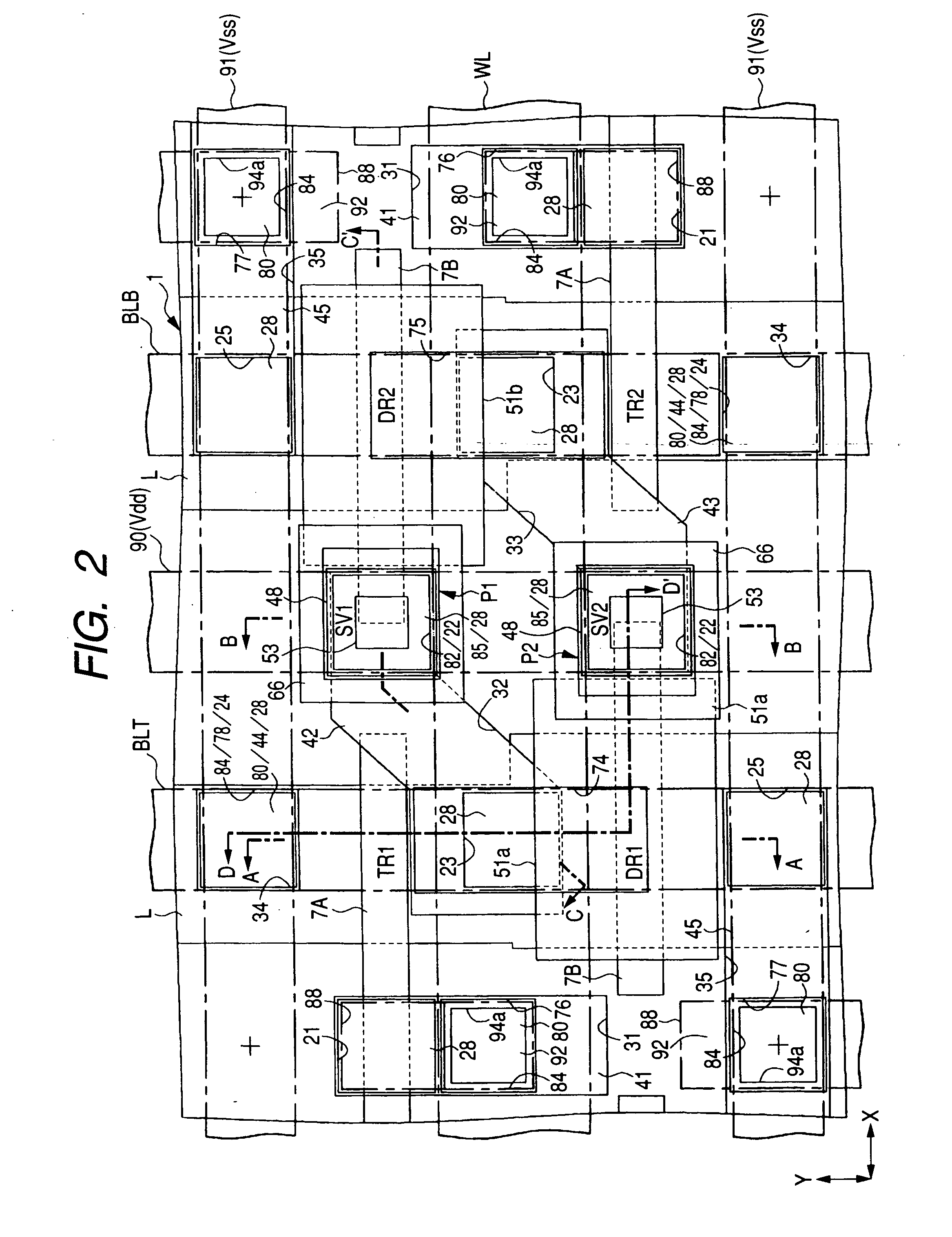
FIG. 1 is an equivalent circuit diagram of a memory cell of a SRAM representing an embodiment according to the present invention. As shown in FIG. 1, a memory cell (MC) of the SRAM has two transfer MISFETs (TR1, TR2), two driving MISFETs (DR1, DR2) and two vertical MISFETs (SV1, SV2) located at the intersection between a pair of complementary data lines (BLT, BLB) and a word line (WL).

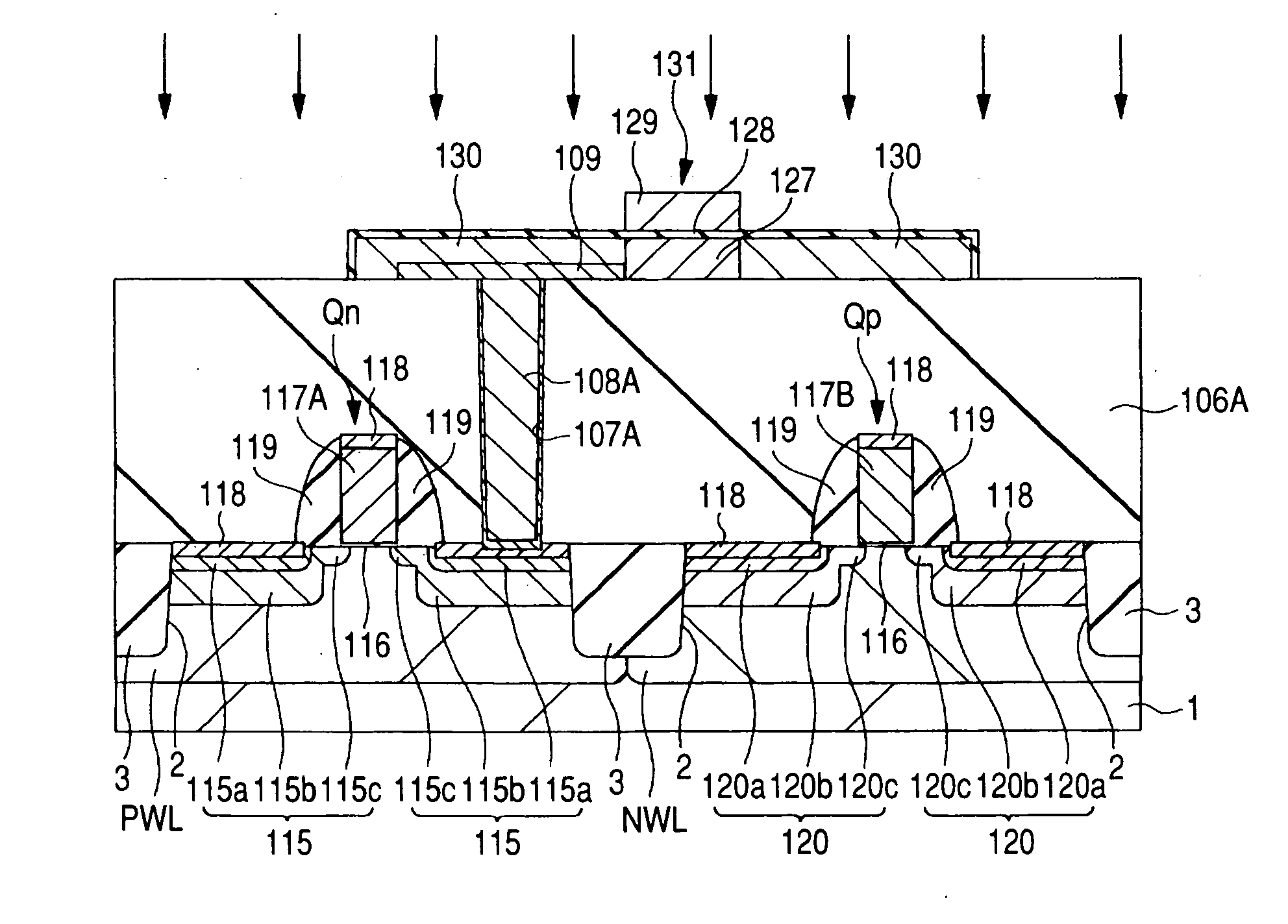
Among the six MISFETs constituting the memory cell (MC), each of the two transfer MISFETs (TR1, TR2) and two driving MISFETs (DR1, DR2) has an n-channel type MISFET. Further, each of the two vertical type MISFETs (SV1, SV2) has a p-channel type MISFET. While the vertical MISFETs (SV1, SV2) correspond to the load MISFET in a well-known complete CMOS type SRAM, as opposed to the usual load MISFET, they are constituted each with a vertical structure, as will be described later, and they are located over the region for forming the driving MISFETs (DR1, DR2) and the transfer MISFETs (TR1, TR...

embodiment 2

(Embodiment 2)

In connection with this Embodiment 2, the description will be directed to a case of applying the invention, for example, to a manufacturing method for manufacture of a DRAM with reference to FIG. 1 to FIG. 13. FIG. 11 to FIG. 13 are cross sectional views showing a main portion of a semiconductor wafer during manufacturing steps in this Embodiment 2.

FIG. 11 shows a cross sectional view showing a main portion of a p-type substrate 1 constituting a semiconductor wafer during steps for manufacture of the DRAM. An n-channel type MISFET Qns for memory cell selection is formed in an active region of the substrate 1. The MISFET Qns has a pair of n-type semiconductor regions 101 for source and drain, a gate insulation film 102 and a gate electrode 103. Phosphorus (P) or arsenic (As) is, for example, introduced to an n-type semiconductor region 101 formed in a p-type well PWL. A gate insulation film 102 formed on the main surface of the substrate 1 is formed, for example, of a...

embodiment 7

(Embodiment 7)

In connection with this Embodiment 7, the description will be directed to an example of the countermeasure taken for the problem arising in a case of providing first and second conductor layers on a metal interconnection.

FIG. 30 shows a diagram which illustrates the problem found for the first time by the present inventors. A metal interconnection 152 comprising, for example, tungsten as a main interconnection material is formed inside an interconnection trench 151 formed in an insulation film 150 by CMP or the like. In the process of forming a conductor layer 48 over the metal interconnection 152 as explained for Embodiment 1, it has been found according to the experiment conducted by the present inventors that a second semiconductor layer comprising, for example, tungsten silicide does not grow smoothly without applying treatment to the surface of the metal interconnection 152 (exposed surface, CMP surface), but small clumps 48b1 of tungsten silicide or the like ar...


PUM

PropertyMeasurementUnit
conduction typeaaaaaaaaaa
sizeaaaaaaaaaa
temperatureaaaaaaaaaa

Abstract

In a semiconductor device, the ohmic contact at the junction between the metal interconnection and the semiconductor layer is lowered by depositing a first conductor layer comprised of, for example, tungsten nitride and a second conductor layer comprised of, for example, tungsten silicide successively from the lower layer so as to cover the upper surface of intermediate conductive layers comprised of a metal, for example, tungsten as a main interconnection material, subsequently introducing an impurity, for example, boron (b) to the second conductor layer, then patterning the first and the second conductor layers thereby forming a conductor layer, and then forming a lower semiconductor layer comprised of, for example, polycrystal silicon for forming a semiconductor region for source and drain of load MISFET of SRAM so as to be in contact with the conductor layer.

Description

CROSS-REFERENCE TO RELATED APPLICATION The present application claims priority from Japanese Patent application No. 2003-319727, filed on Sep. 11, 2003, the content of which is hereby incorporated by reference into this application. BACKGROUND OF THE INVENTION The present invention concerns a semiconductor device and a method of manufacture thereof; and, more in particular, it relates to a technique which is effective for application to the manufacture of a semiconductor device having an SRAM (Static Random Access Memory) in which a memory cell is constituted by using vertical-type MISFETs. In an SRAM which represents a kind of general-purpose large capacity semiconductor memory device, a memory cell is constituted, for example, with four n-channel type MISFETs (Metal-Insulator-Semiconductor-Field-Effect-Transistor) and two p-channel type MISFETs. However, in the so-called complete CMOS (Complementary-Metal-Oxide-Semiconductor) type SRAM of this type, since six MISFETs are arrang...

Claims


Application Information

Patent Timeline
Patent Type & Authority Applications(United States)
IPC IPC(8): H01L21/28H01L23/52H01L21/3205H01L21/44H01L21/768H01L21/822H01L21/8234H01L21/8238H01L21/8242H01L21/8244H01L27/00H01L27/04H01L27/08H01L27/088H01L27/092H01L27/108H01L27/11
CPCH01L21/76838H01L27/11H01L27/10888H01L27/10855H01L27/0688H10B12/0335H10B12/485H10B10/00H01L21/28
Inventor NISHIDA, AKIOICHINOSE, KAZUHITOCHAKIHARA, HIRAKU
Owner RENESAS TECH CORP
Why Eureka
Try Eureka