Semiconductor memory device and various systems mounting them

a memory device and semiconductor technology, applied in semiconductor devices, digital storage, instruments, etc., can solve the problems of long read/write access time, electrode operation with a large load capacity, polarization characteristics have a hysteresis,

Inactive Publication Date: 2005-03-24
TOSHIBA MEMORY CORP
View PDF10 Cites 25 Cited by
  • Summary
  • Abstract
  • Description
  • Claims
  • Application Information

AI Technical Summary

Benefits of technology

It is an object of the present invention to provide a semiconductor memory device which can realize a memory cell having a size (e.g. 4F2) smaller than 8F2 without using any stacked-type transistor or the like and also maintain a random access function.
As described above in detail, the present invention makes it possible to provide the following advantages: easy production is available by using nonvolatile planar transistors, high integrity having a size of 4F2 is realized with random access properties, and (1) in the 1T / 1C type, the plate driving scheme is adopted, which makes it possible to carry out a high-density operation with low voltage. Moreover, (2) high-speed operation is achieved while suppressing dispersion in the paraelectric component in the ferroelectric capacitor. Furthermore, (3) noise at the time of writing is reduced. (4) High-speed operation is achieved in the plate driving scheme while reducing process costs and chip sizes. (5) Since cells are formed by using CMOS, it is possible to eliminate voltage raising processes to the word line and the block selection line.

Problems solved by technology

In the FRAM, however, the polarization characteristics have a hysteresis.
Accordingly, a plate electrode operation with a large load capacity is required, and read / write access takes a long time.
This is the disadvantage of the FRAM.
On the other hand, the scheme shown in FIG. 3B or 3C is more disadvantageous than that shown in FIG. 3A in that the voltage (coercive voltage Vc) necessary for polarization inversion must be (½)Vcc or less (this problem is solved by reducing the size of the ferroelectric film).
Additionally, the FRAM has a large disadvantage in that a refresh operation is required, like the DRAM (the refresh operation increases the stand-by current or generates a busy rate).
In the scheme for driving the plate electrode between 0V and Vdd, a lot of memory cells are connected to the plate electrode, causing a large load capacity and a very long driving time; therefore, as compared with the conventional DRAM, the operations become slow in both access time and cycle time.
Consequently, when “1” data is maintained in the SN, the SN drops to Vss due to the junction leakage at the p-n junction, with the result that cell information is destroyed in the case of the plate electrode fixed to (½)Vdd.
Therefore, in the (½)Vdd cell plate scheme, the refresh operation is required, resulting in the problem of power increase and the difficulty in production due to severe cell specifications.
As described above, the first problem with the conventional FRAM is that it is difficult to simultaneously achieve high-speed operations (PL potential fixed) and the omission of the refresh.
The FRAM also has the same problems as those of the DRAM.
The stacked-type transistor or stacked-type TFT can hardly be realized because the manufacturing process is more complex than that for a conventional planar transistor having a size of 8F2, which can be easily manufactured.
Additionally, the conventional FRAM cannot simultaneously realize the high-speed operation of the scheme of fixing the plate electrode potential and omission of the refresh operation.
Consequently, the second problem with the conventional FRAM cell is that it is impossible to simultaneously achieve the following three points: (1) memory cells having a small size of 4F2, (2) planar transistors that are easily manufactured and (3) general-purpose random access function.
However, the ferroelectric capacitor has great dispersion in its paraelectric component due to dispersion in manufacturing processes, etc.
; and this degrades the read-out margin to a great degree.
However, in this scheme, as shown in FIG. 4C, PL is again raised, and then PL is lowered in order to re-write data; consequently, PL has to be raised and lowered twice, with the result that read / write access and cycle take a very long time as compared with the case shown in FIG. 4B.
As described above, in the conventional FRAM, the first problem is that it is difficult to achieve both of the high-speed operation (PL potential fixed) and the omission of the refresh operation, and the second problem is that it is impossible to simultaneously achieve the following three points: memory cells having a small size of 4F2, planar transistors that are easily manufactured and general-purpose random access function.
Moreover, when an attempt is made to suppress dispersion in the paraelectric component of a ferroelectric capacitor, the operation tends to become slow.
However, such examinations have not reached a practical level yet because of the above-described problems unique to the FRAM.

Method used


Image

  • Semiconductor memory device and various systems mounting them
  • Semiconductor memory device and various systems mounting them
  • Semiconductor memory device and various systems mounting them

Examples


first embodiment

(First Embodiment)

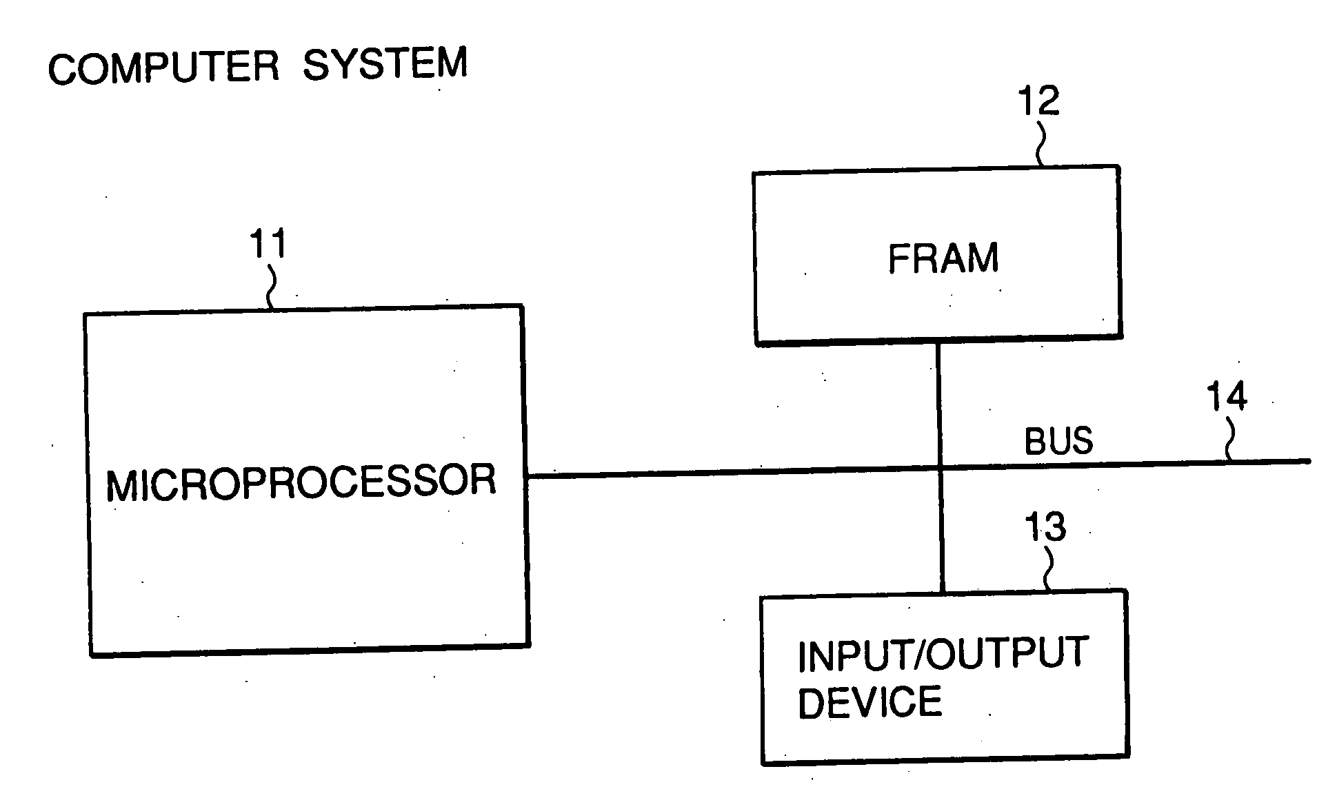
FIG. 5 is a block diagram showing the basic structure of a computer system according to the first embodiment of the present invention;

This system is constituted by a microprocessor 11 for performing various arithmetic processing operations, a nonvolatile semiconductor memory device 12 connected to the microprocessor 11 through a bus 14 to store data, and an input / output device 13 connected to the microprocessor 11 through the bus 14 to transmit / receive data to / from an external device.

In this embodiment, the semiconductor memory device (FRAM) of the present invention is mounted in the computer system. The FRAM used in this embodiment will be described below in detail.

FIG. 6A and FIG. 6B are circuit diagrams showing the basic structure of the FRAM used in this embodiment.

FIG. 6A and FIG. 6B show an equivalent circuit corresponding to eight memory cells. Referring to FIG. 6A, reference symbol BL denotes a bit line; PL, a plate electrode; WLij, a word line; and S...

second embodiment

(Second Embodiment)

FIG. 9 is a block diagram showing the basic structure of a computer system according to the second embodiment. The same reference numerals as in FIG. 5 denote the same parts in FIG. 9, and a detailed description thereof will be omitted.

In this embodiment, a controller 15 for controlling an FRAM 12 is added to the structure shown in FIG. 5. More specifically, the FRAM 12 is connected to a bus 14 through the controller 15.

In this structure as well, the same effects as in the first embodiment can be obtained. The controller 15 of this embodiment allows to omit a refresh control signal generation circuit, so that the cost can be reduced.

third embodiment

(Third Embodiment)

FIG. 10 is a block diagram showing the basic structure of a computer system according to the third embodiment. The same reference numerals as in FIG. 9 denote the same parts in FIG. 10, and a detailed description thereof will be omitted.

This embodiment is different from the second embodiment in that the I / O of an FRAM 12 is directly connected to a system bus 14. The system can be freely constituted.

In this structure as well, the same effects as in the first embodiment can be obtained. A controller 15 of this embodiment allows to omit a refresh control signal generation circuit, so that the cost can be reduced.


PUM


Abstract

A semiconductor memory device comprises a plurality of memory cells each having a source terminal and a drain terminal and a ferroelectric capacitor having a first terminal connected to the source terminal, wherein the plurality of memory cells are connected in series, and one or more selected transistors connected to at least one terminal of the series connected memory cells to constitute a memory cell block, the memory cell block having one terminal connected to a bitline and another terminal connected to a plate electrode, and wherein two memory cell blocks, which are respectively connected to two bit lines forming a bit line pair and also connected to the same word line, are respectively connected to a first plate electrode and a second plate electrode.

Description

BACKGROUND OF THE INVENTION The present invention relates to a semiconductor memory device, especially, to a nonvolatile semiconductor memory device using a ferroelectric capacitor, a method of driving the same, and various systems each having the semiconductor memory device. In recent years, a nonvolatile memory (FRAM) using a ferroelectric capacitor has received a great deal of attention as one of semiconductor memories. Since the FRAM is advantageous in that it is nonvolatile, the number of times of rewrite access is 1012, the read / write time almost equals that of a DRAM, and it can operate at a low voltage of 3 to 5V, the FRAMs may replace all memory markets. At present, in the Society, 1M bit FRAMs have been reported. (H. Koike et al., 1996, IEEE International Solid-State Circuit Conference Digest of Technical Paper, pp. 368-369, February, 1996). Along with developments, the cell size of the FRAM has been reduced by simplifying and micropatterning the cell structure, as in d...

Claims


Application Information

Patent Timeline
Patent Type & Authority Applications(United States)
IPC IPC(8): G11C11/22G11C11/56H01L27/115
CPCG11C11/22H01L27/11502G11C11/5657H10B53/00
Inventor TAKASHIMA, DAISABURO
Owner TOSHIBA MEMORY CORP
Why Eureka
Try Eureka