Method and apparatus for forming low permittivity film and electronic device using the film

Inactive Publication Date: 2005-03-24
SUGINO TAKASHI +2
View PDF3 Cites 3 Cited by
  • Summary
  • Abstract
  • Description
  • Claims
  • Application Information

AI Technical Summary

Benefits of technology

Moreover, the film formation method of the present invention for achieving the above object, after forming the film, can include the performance of an infrared lighting step using an infrared lamp to thereby heat the thin film. Setting this holding temperature at 250° C

Problems solved by technology

However, with the increasing integration of transistors, the problem has arisen of wiring delays occurring due to the volume between wirings, which is a factor in inhibiting high speed electronic switching operations.
Given this situation, although organic materials and porous materials have gained attention and make realization of an extremely low dielectric constant (dielectric constant of κ˜2.5 or less) possible, chemically there are problems in terms of

Method used


Image

  • Method and apparatus for forming low permittivity film and electronic device using the film
  • Method and apparatus for forming low permittivity film and electronic device using the film
  • Method and apparatus for forming low permittivity film and electronic device using the film

Examples


embodiment 1

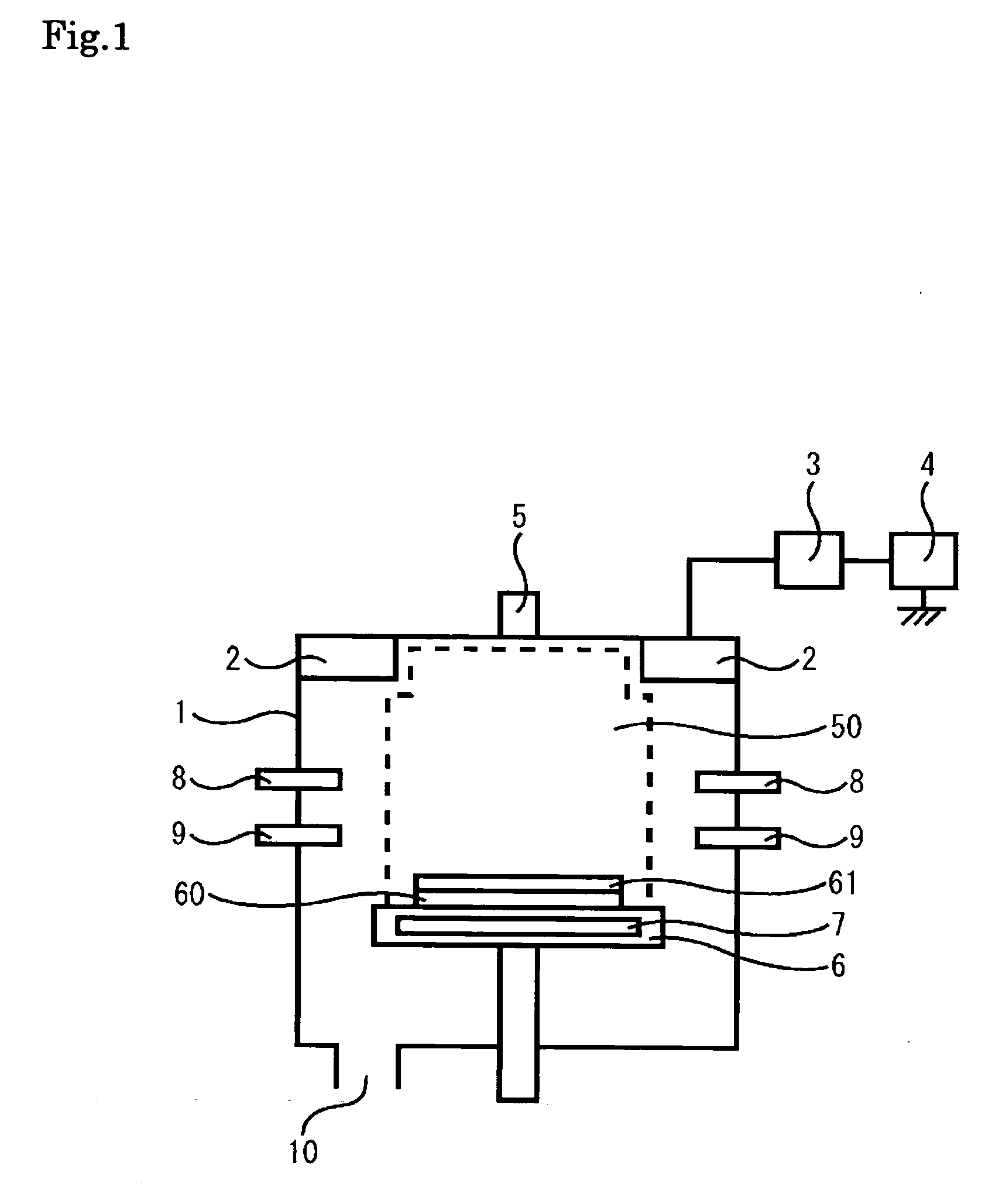
FIG. 1 is a schematic side view showing the film formation apparatus for implementing the film formation method of a first embodiment of the present invention. A dielectric binding plasma generating section 2 is provided in a cylindrical housing 1 and is connected to a high frequency power supply 4 via a matching unit 3.

The high frequency power supply 4 can supply high frequency power of up to 1 to 10 kw. Nitrogen gas is supplied from the nitrogen gas introduction section 5 to produce plasma 50. The substrate 60 is placed in the substrate holding section 6, and the heater 7 is installed in the substrate holding section 6. The temperature of the substrate 60 can be set within a range from room temperature to 600° C. by the heater 7. In the cylindrical container 1, the introduction section 8 for introducing boron chloride gas with hydrogen gas as a carrier is provided.

Also, an introduction section 9 for introducing a hydrocarbon gas into the cylindrical container 1 is provided. An...

embodiment 2

The second embodiment of the present invention uses the same film formation apparatus as the first embodiment. A dielectric binding plasma generating section 2 is provided in a cylindrical housing 1 and is connected to a high frequency power supply 4 via a matching unit 3.

The high frequency power supply 4 can supply high frequency power of 1 to 10 kw. Nitrogen gas is supplied from the nitrogen gas introduction section 5 to produce plasma 50. The substrate 60 is placed in the substrate holding section 6, and the heater 7 is installed in the substrate holding section 6. The temperature of the substrate 60 can be set within a range from room temperature to 600° C. by the heater 7.

In the cylindrical container 1, the introduction section 8 for introducing boron chloride gas with hydrogen gas as a carrier is provided. Also, an introduction section 9 for introducing a hydrocarbon gas into the cylindrical container 1 is provided. An exhaust section 10 is installed under the substrate h...

embodiment 3

FIG. 4 is a schematic side view showing the film formation apparatus for implementing the film formation method of a third embodiment of the present invention. A dielectric binding plasma generating section 2 is provided in a cylindrical housing 1, and is connected to a high frequency power supply 4 via a matching unit 3.

The high frequency power supply 4 can supply high frequency power of up to 1 to 10 kw. Nitrogen gas is supplied from the nitrogen gas introduction section 5 to produce plasma 50. The substrate 60 is placed in the substrate holding section 6 and the heater 7 is installed in the substrate holding section 6. The temperature of the substrate 60 can be set within the range from room temperature to 600° C. by the heater 7.

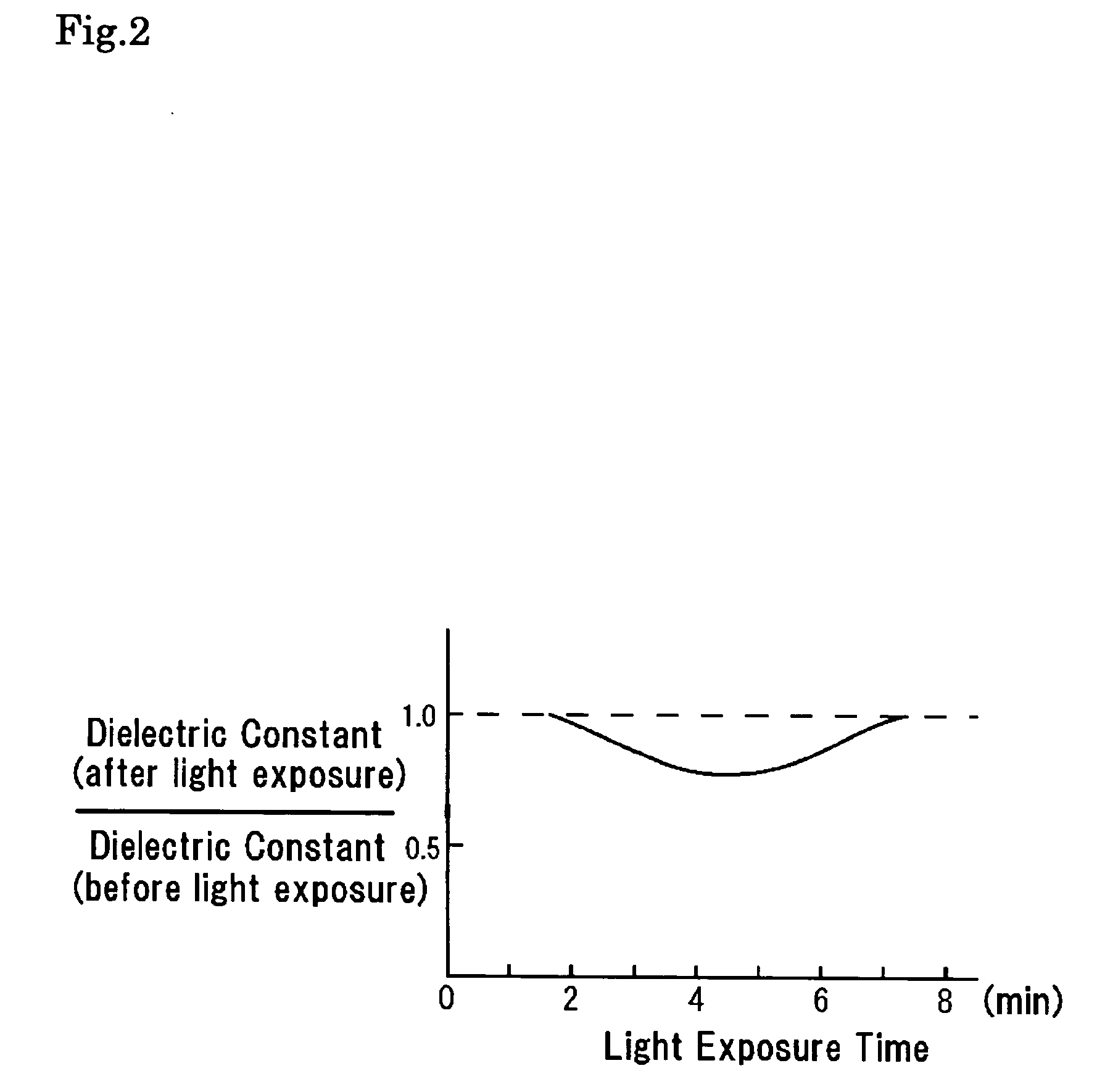
Further, a window is provided in the top of the substrate holding section of the film formation chamber, so that the surface of the sample can be illuminated by a mercury lamp. When illuminated by the mercury lamp, the substrate holding section 6 can...


PUM

PropertyMeasurementUnit
Dielectric constantaaaaaaaaaa
Permittivityaaaaaaaaaa

Abstract

A film formation method enables the creation of a low dielectric constant boron-carbon-nitrogen thin film. The film formation method includes the steps of generating plasma in a film formation chamber, reacting boron and carbon with nitrogen atoms inside the film formation chamber, forming a boron-carbon-nitrogen film on a substrate, and thereafter subjecting the formed film to light exposure (e.g., ultraviolet and/or infrared).

Description

BACKGROUND OF THE INVENTION 1. Field of the Invention The present invention relates to a film formation method for producing a film that includes boron, carbon, and nitrogen, and an electronic device that utilizes the same. 2. Description of the Related Art Until now SiO2 and SiN films formed by the plasma CVD (chemical vapor deposition) method have been used as wiring interlayer insulation thin films and protection films in semiconductor integrated circuits. However, with the increasing integration of transistors, the problem has arisen of wiring delays occurring due to the volume between wirings, which is a factor in inhibiting high speed electronic switching operations. Also, there is a demand for improving the wiring delay in liquid crystal display panels. Lowering the dielectric constant of wiring interlayer insulation thin films is necessary in order to solve this problem, and a new material having a low dielectric constant is required for interlayer insulation films. Giv...

Claims


Application Information

Patent Timeline
IPC IPC(8): C23C16/30C23C16/36H01L21/318H01L21/768
CPCC23C16/30C23C16/36H01L21/318H01L21/76835H01L21/76828H01L21/76829H01L21/76801H01L21/02112H01L21/02345H01L21/02348
Inventor SUGINO, TAKASHIKUSUHARA, MASAKIUMEDA, MASARU
Owner SUGINO TAKASHI
Why Eureka
Try Eureka