Method for micro-roughening treatment of copper and mixed-metal circuitry

a technology of mixed metals and metal layers, which is applied in the direction of printed circuit manufacturing, printed circuit aspects, and the improvement of the adhesion of metals to the insulating substrate, etc. it can solve the problems of unbalanced etching effect of mixed metal layers, unbalanced etching of copper micro-roughening, and inability to properly micro-roughen copper in the area of circuit elements adjacent to the mixed metal interface, so as to enhance the adhesion properties of metal patterns

Inactive Publication Date: 2005-03-31
ATOTECH DEUT GMBH
View PDF18 Cites 57 Cited by
  • Summary
  • Abstract
  • Description
  • Claims
  • Application Information

AI Technical Summary

Benefits of technology

In one embodiment, the process further comprises a step of pre-cleaning the first major surface. An additional preconditioning step may be added between the pre-cleaning step and step (b) to enhance the uniformity of the treatment in step (b). Additional treatment steps may be added between steps (g) and (h) to further enhance the adhesion properties of the metal pattern to the dielectric material without substantially modifying the underlying metal structure. An additional step may be added between steps (b) and (c) or between steps (f) and (g) to chemically adjust the color of the micro-roughened surface in order to aid optical inspection.
The process in accordance with the present invention is simpler and shorter (i.e., includes fewer steps) than a typical circuit patterning sequence. Treating the copper surface is carried out by bringing the copper surface into contact with the appropriate solutions. Optical inspection may be performed manually or automatically. Copper-Invar-copper layers treated in accordance with the invention have a uniformly micro-roughened upper surface with none of the original copper color visible to the naked eye. In mixed-metal embodiments, in the present invention, the area of non-roughening is restricted to a narrow band along the outer edges of the unpatterned layer or panel. This area is normally trimmed away and not used in the final product. Adhesion of the micro-roughened metal surfaces to subsequently applied dielectric material is not problematic (no peeling or blistering). In embodiments in which the optional metal coating is applied by step (g), the adhesion is further enhanced, and even the side walls of the circuitry (which in one embodiment are not micro-roughened) have improved adhesion to the dielectric layer. As a result of the process of the present invention, the cross-sectional area of a patterned circuit made with mixed-metal or copper is not significantly reduced after step (e). Overall, there are fewer process steps required to create a patterned circuit layer with improved adhesion to dielectric material. The described process is therefore advantageous for manufacturing multilayer printed circuit boards.

Problems solved by technology

Due to the high temperatures required for this process, the hazardous nature of the chemicals used, and the fragile quality of the oxide crystals deposited on the copper surface, alternative roughening methods have replaced the black oxide process in many circuit board manufacturing facilities.
As noted below, the quantity of metal removed from the already-formed circuit pattern elements 102 may have undesirable effects upon the function of the circuit pattern due to the total quantity of metal removed.
With certain copper micro-etching processes, such as sulfuric acid / hydrogen peroxide solutions containing organic additives, mixed-metal layers create an unbalanced etching effect where the interface of two different metals comes into contact with the treatment solution.
In the case of copper-Invar-copper, the Invar is less corrosion-resistant than the copper, and this prevents the copper from being properly micro-roughened in the areas of the circuit elements adjacent to the mixed-metal interface.
As a result, the adhesion of dielectric material to the copper pattern may be poor since the adhesion has not been improved due to the unsuccessful micro-roughening.
However, in the case of mixed metals, the surface of the etched patterns remain the color of untreated copper.
Any such untreated copper surface is undesirable and may require the product to be scrapped due to poor adhesion of the metal to later-applied laminate materials.
This process greatly increases surface roughness, but may result in other problems, such as resist lock-in.
This is a situation where the etch resist is trapped in the deep crevices of the foil treatment and cannot be easily developed or stripped.
The locked-in resist can cause defects such as electrical shorts.
In general, the type of surface treatment provided on mixed-metal foil is adequate for dielectric adhesion, but problematic for etch resist patterning and removal.
Another limitation of the state of the art is the large number of process steps used to pattern a metal layer.
Another problem in the conventional process of etching followed by micro-roughening results from the total quantity of metal removed from the circuit pattern during the micro-roughening of pre-formed or pre-patterned circuit elements.
This loss in cross-sectional area reduces the current-carrying capacity of the circuit element, thus increasing the resistance thereof.
This can create significant problems for the ever-smaller circuitry, since the conventional solution to this problem requires forming larger circuit elements to compensate for the loss of metal in subsequent micro-roughening.
Thus, as described above with respect to FIG. 2, when the edge effect occurs, significant portions of the top layer 410 are left un-roughened, thus compromising effective adhesion to subsequently applied dielectric materials.
In typical circuit patterning processes such as that outlined above for single-metal layers, it is not possible to simply skip the micro-roughening step (9) because the surface roughness created by the micro-etching step (2) is insufficient to allow reliable adhesion of the dielectric layer.
In the mixed-metal layer embodiments, it is not possible to obtain adequate roughening and as a result may not be possible to obtain adequate adhesion of the metal to later-applied laminate materials due to the edge effects described.
Thus, since the micro-etch roughness is usually not sufficient to enhance adhesion to subsequently applied dielectric laminate materials, the micro-roughening needs to be included.
However, doing so may result in loss of a substantial amount of the circuit pattern cross-sectional area.
If the circuit pattern elements are made larger initially to compensate for this later loss, the sought reduction in overall circuit pattern size cannot be obtained, thus inhibiting needed size reductions.

Method used


Image

  • Method for micro-roughening treatment of copper and mixed-metal circuitry
  • Method for micro-roughening treatment of copper and mixed-metal circuitry
  • Method for micro-roughening treatment of copper and mixed-metal circuitry

Examples


first embodiment

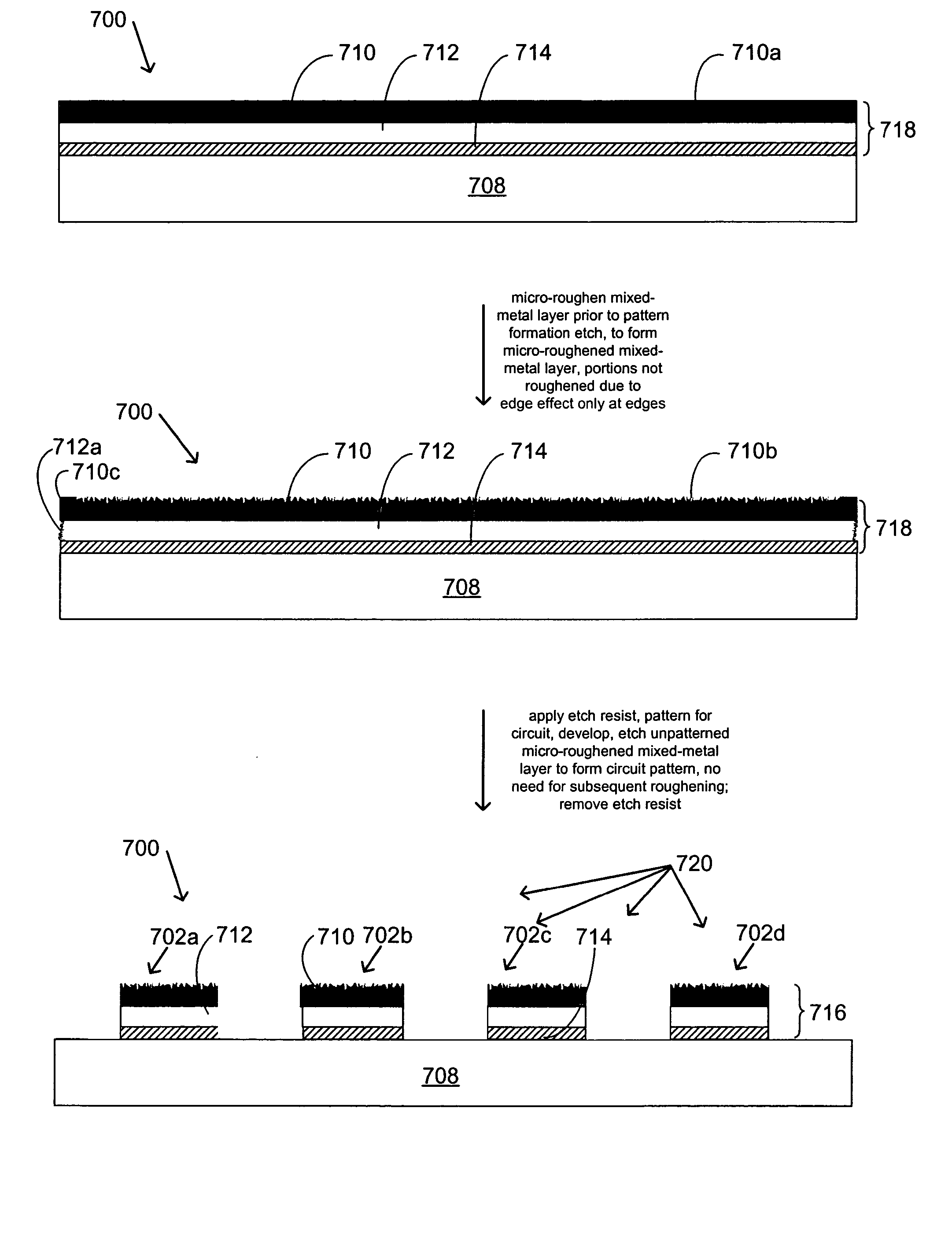
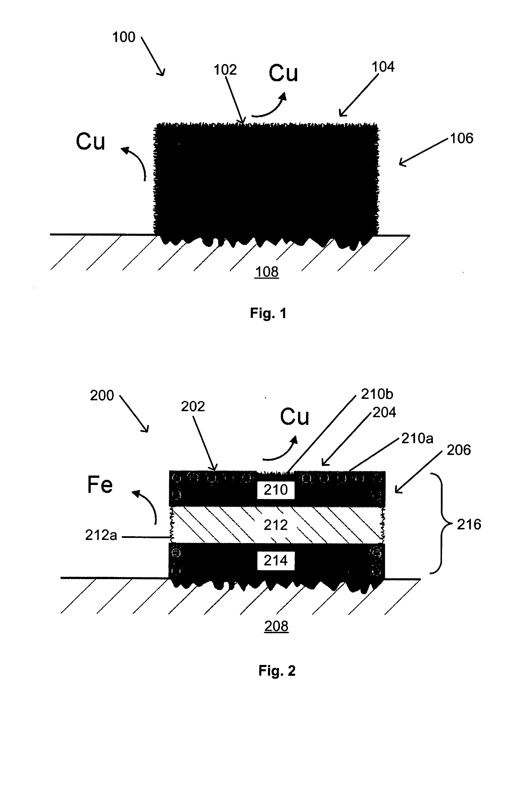
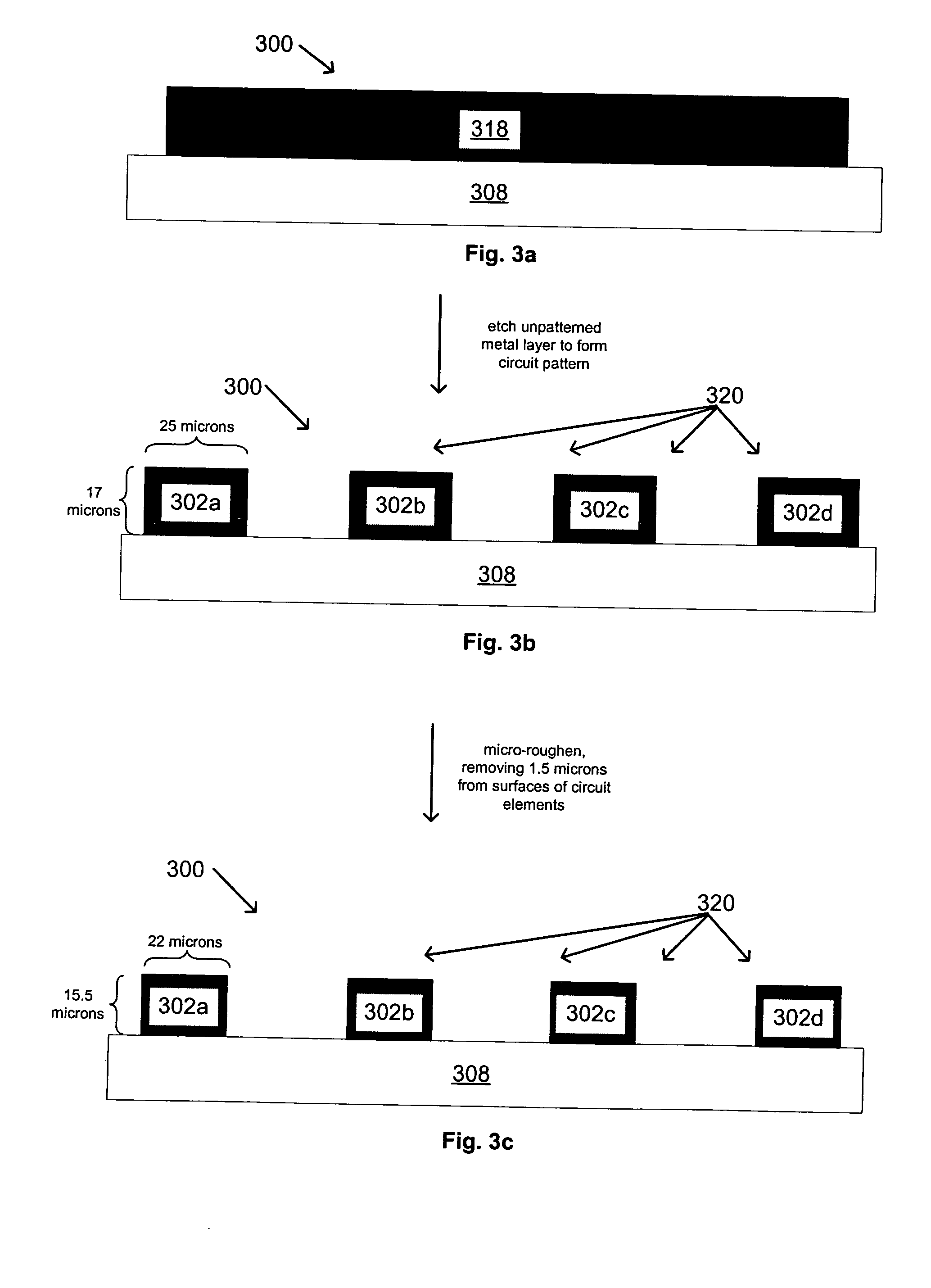
In the first embodiment, the invention relates to a process to improve adhesion of dielectric materials to a metal layer, including providing an unpatterned metal layer having a first major surface; micro-roughening the first major surface to form a micro-roughened surface; and etching the metal layer to form a circuit pattern in the metal layer, in which the micro-roughening is carried out prior to the etching. In one embodiment, prior to the micro-roughening, no surface treatment to increase the roughness of the metal layer is carried out. In one embodiment, no further surface treatment to increase the roughness of the metal is carried out subsequent to the etching to form the circuit pattern.

In the second embodiment, the invention relates to a process to improve adhesion of dielectric materials to a metal layer, comprising: a. providing an unpatterned metal layer having a first major surface; b. micro-roughening the unpatterned metal layer with a solution to form a micro-rough...

third embodiment

In the present invention, additional steps are included, specifically, a dielectric material layer is applied, and optionally, a metal layer may be applied to further enhance adhesion to the dielectric material.

The steps (a)-(f) of the third embodiment may be substantially the same as those described above with respect to the second embodiment.

In the next step (h) of the third embodiment of the process of the present invention, a dielectric material layer is applied to the micro-roughened surface of the circuit pattern. After rinsing and drying, the patterned circuit is ready for dielectric application. The surface is already appropriately micro-roughened to have reliable adhesion to dielectric material. However, certain dielectric materials which exhibit poor adhesion to copper may show improved adhesion when a secondary metal is applied by chemical reaction to the surface of the micro-roughened copper. For example, a thin layer of tin may be applied to the copper surface using ...


PUM

PropertyMeasurementUnit
pKaaaaaaaaaaa
surface roughnessaaaaaaaaaa
temperaturesaaaaaaaaaa

Abstract

Process to improve adhesion of dielectric materials to a metal layer, including providing an unpatterned metal layer having a first major surface; micro-roughening the first major surface to form a micro-roughened surface; and etching the metal layer to form a circuit pattern in the metal layer, in which the micro-roughening is carried out prior to the etching.

Description

TECHNICAL FIELD The present invention relates to micro-roughening of metal layers for use in, e.g., circuit boards, and more particularly, to methods for micro-roughening metal layers and mixed-metal layers while avoiding or reducing problems known in the prior art. BACKGROUND OF THE INVENTION In the manufacture of multi-layer circuit boards, it is necessary to use a dielectric material to separate different layers of circuitry. Electrical connections between layers are formed by creating holes in the dielectric material and depositing a conductive material within the hole, which also makes contact with two or more of the circuit layers. A variety of materials exhibit dielectric properties and can be used as a dielectric layer. A few examples include epoxy resin, phenolic resin, polyimide, bismaleimide triazine, and polytetrafluoroethylene. The metal circuitry usually consists of copper that has been patterned by a plating or etching process. In order to prevent delamination betwe...

Claims


Application Information

Patent Timeline
Patent Type & Authority Applications(United States)
IPC IPC(8): C23F1/18H05K3/02H05K3/06H05K3/38H05K3/46
CPCC23F1/18H05K3/022H05K3/064H05K2203/124H05K3/4641H05K2201/0338H05K2201/068H05K3/383H05K3/06
Inventor FUERHAUPTER, HARRYBARON, DAVID THOMASJOHAL, KULDIP SINGHBROOKS, PATRICK PAUL
Owner ATOTECH DEUT GMBH
Why Eureka
Try Eureka