Three dimensional CMOS integrated circuits having device layers built on different crystal oriented wafers

a technology of integrated circuits and crystal oriented wafers, which is applied in the direction of semiconductor devices, semiconductor/solid-state device details, electrical apparatus, etc., can solve the problems of reducing the orientation of nfet devices, reducing the efficiency of nfet devices, and undesirable pfets having larger widths, etc., to achieve improved transistor packing density, reduced chip footprint, and increased packing density

Inactive Publication Date: 2005-03-31
GLOBALFOUNDRIES INC
View PDF22 Cites 288 Cited by
  • Summary
  • Abstract
  • Description
  • Claims
  • Application Information

AI Technical Summary

Benefits of technology

[0012] One advantage of 3D integration is increased packing density; by adding a third dimension to the conventional 2D layout, the transistor packing density can be improved thereby allowing a reduced chip footprint. This is particularly appealing for wireless or portable electronics. Another advantage of 3D i...

Problems solved by technology

To compensate for this discrepancy, pFETs are typically designed with larger widths in order to balance pull-up currents against the nFET pull-down currents and achieve uniform circuit switching pFETs having larger widths are undesirable since they take up a significant amount of chip area.
Unfortunately, electron mobilities on (110) Si surfaces are significantly degraded compared to (100) Si surfaces.
As can be deduced from the above discussion, the (110) Si surface is optimal for pFET devices because of excellent hole mobility, yet such a crystal orientation is completely inappropriate for nFET devices.
It is becoming more difficult to achieve substantial integrated circuit (IC) performance enhancement by traditional CMOS device and interconnect scaling.
New materials introduced into the front-e...

Method used


Image

  • Three dimensional CMOS integrated circuits having device layers built on different crystal oriented wafers
  • Three dimensional CMOS integrated circuits having device layers built on different crystal oriented wafers
  • Three dimensional CMOS integrated circuits having device layers built on different crystal oriented wafers

Examples


Embodiment Construction

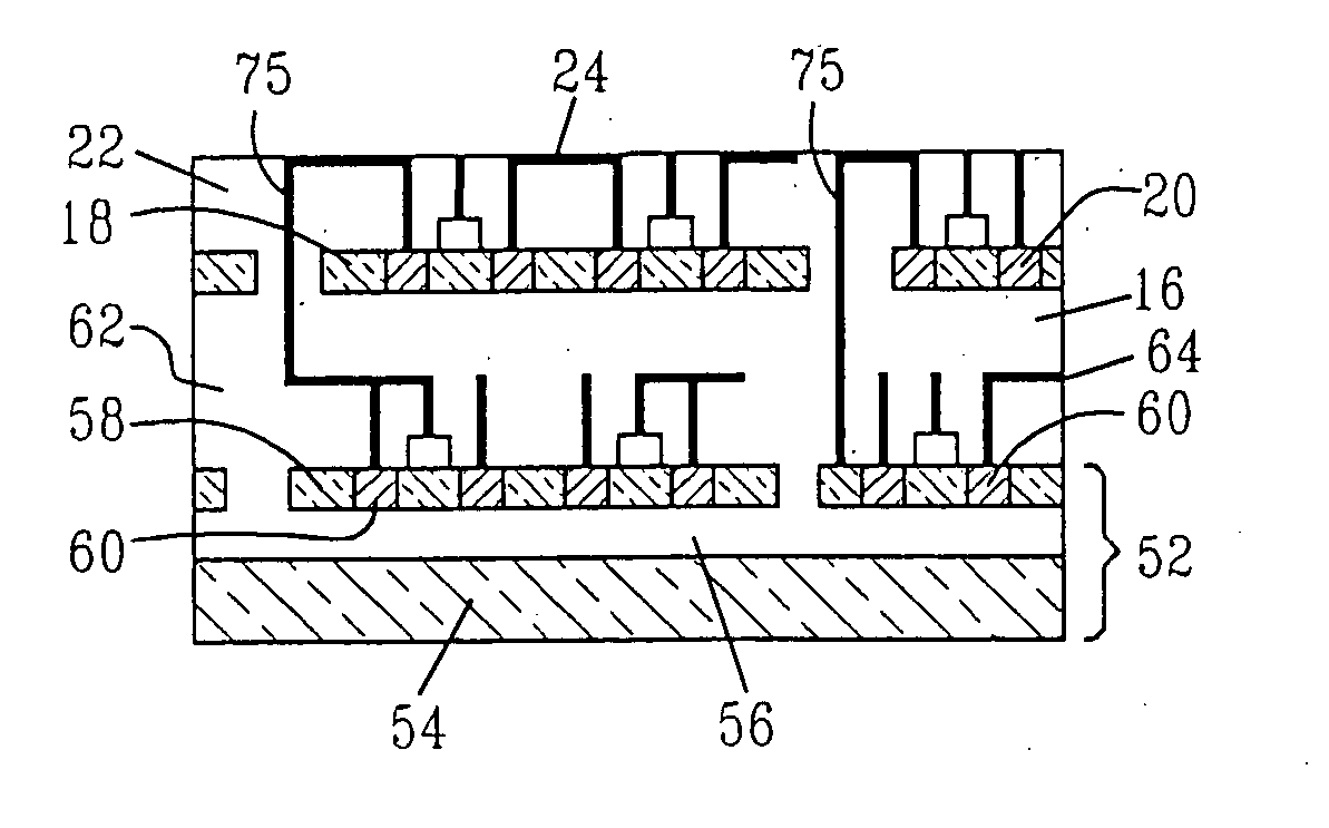
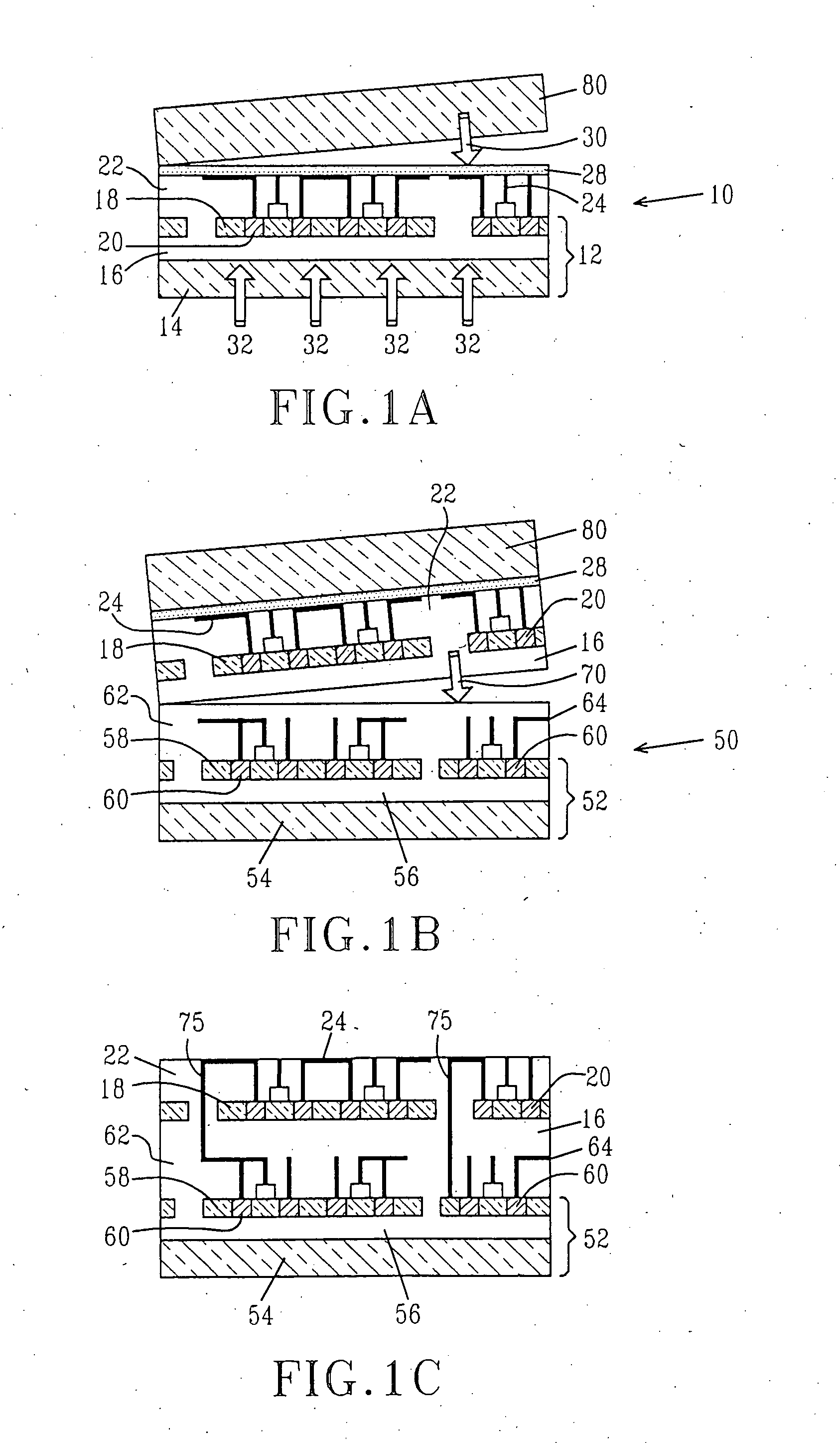
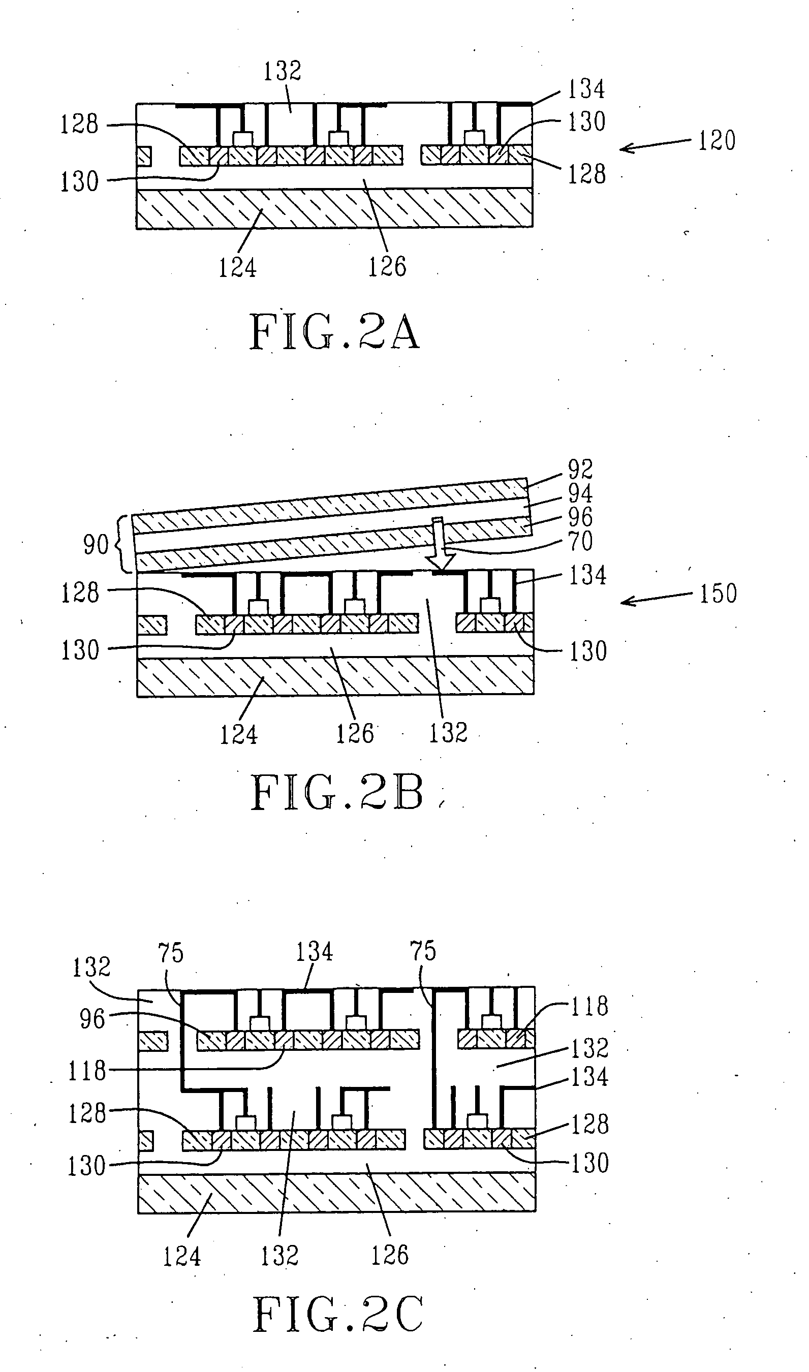
[0031] The present invention, which provides 3D integration schemes for forming a 3D CMOS integrated circuit having device layers built on different crystal oriented SOI wafers, will now be described in greater detail by referring to the drawings that accompany the present invention. In the accompanying drawings, like and / or corresponding elements are referred to by like reference numerals.

[0032] In the present invention, the terms “silicon-on-insulator” or “SOI” wafer (the term ‘substrate’ can interchangeable used with the term ‘wafer’) are used to define a semiconductor structure in which a buried insulating layer, such as a buried oxide layer, separates a top Si-containing layer (also referred to as the SOI layer or the device layer) from a bottom Si-containing substrate layer. The term “Si-containing” is used in the present invention to denote a semiconductor material that includes silicon. Illustrative examples of such Si-containing materials include, but are not limited to: S...


PUM


Abstract

Three-dimensional (3D) integration schemes of fabricating a 3D integrated circuit in which the pFETs are located on an optimal crystallographic surface for that device and the nFETs are located on a optimal crystallographic surface for that type of device are provided. In accordance with a first 3D integration scheme of the present invention, first semiconductor devices are pre-built on a semiconductor surface of a first silicon-on-insulator (SOI) substrate and second semiconductor devices are pre-built on a semiconductor surface of a second SOI substrate. After pre-building those two structures, the structure are bonded together and interconnect through wafer-via through vias. In a second 3D integration scheme, a blanket silicon-on-insulator (SOI) substrate having a first SOI layer of a first crystallographic orientation is bonded to a surface of a pre-fabricating wafer having second semiconductor devices on a second SOI layer that has a different crystallographic orientation than the first SOI layer; and forming first semiconductor device on the first SOI layer.

Description

FIELD OF THE INVENTION [0001] The present invention relates to complementary metal oxide semiconductor (CMOS) integrated circuits, and more particularly to three-dimensional CMOS integrated circuits having semiconductor device layers that are built on different crystal oriented wafers. BACKGROUND OF THE INVENTION [0002] In present semiconductor technology, CMOS devices, such as nFETs or pFETs, are typically fabricated upon semiconductor wafers, such as Si, that have a single crystal orientation. In particular, most of today's semiconductor devices are built upon Si having a (100) crystal orientation. [0003] Electrons are known to have a high mobility for a (100) Si surface orientation, but holes are known to have high mobility for a (110) surface orientation. That is, hole mobility values on (100) Si are roughly 2×-4× lower than the corresponding electron hole mobility for this crystallographic orientation. To compensate for this discrepancy, pFETs are typically designed with larger...

Claims


Application Information

Patent Timeline
IPC IPC(8): H01L21/02H01L21/336H01L27/08H01L21/68H01L21/8238H01L23/52H01L27/00H01L27/06H01L27/085H01L27/092H01L27/12H01L29/786
CPCH01L21/6835H01L25/0657H01L27/0688H01L27/1203H01L2924/0002H01L2221/68368H01L2924/00H01L27/085
Inventor CHAN, VICTORGUARINI, KATHRYN W.IEONG, MEIKEI
Owner GLOBALFOUNDRIES INC
Why Eureka
Try Eureka