Antistatic conductive grid pattern with integral logo

a grid pattern and antistatic technology, applied in thermography, instruments, photosensitive materials, etc., can solve the problems of increased brittleness, physical defects, loss of antistatic function, etc., and achieve the effect of reducing material costs, improving image processing equipment, and reducing coverag

Inactive Publication Date: 2005-03-31
EASTMAN KODAK CO
View PDF15 Cites 29 Cited by
  • Summary
  • Abstract
  • Description
  • Claims
  • Application Information

AI Technical Summary

Benefits of technology

The present invention includes several advantages, not all of which are incorporated in a single embodiment. Coating the antistatic layer in a patterned format provides a network of conductive pathways at a significantly reduced coverage (up to 80-90% reduction). The pattern may be a simple grid pattern or any other interconnected labyrinthine pattern. The significant reduction in coverage of the antistatic layer of the invention leads directly to savings in material costs. Significantly less conductive material may be required to provide antistatic protection, friction control and improved transport through image processing equipment. The conduc

Problems solved by technology

The problem of controlling static charge during plastic web manufacturing and transport is well known.
Generation and uncontrolled discharge of electrostatic charge can cause a number of serious problems including safety hazards.
In the field of imaging, particularly photography, the accumulation of charge on film or paper surfaces leads to the attraction of dirt, which can produce physical defects.
However, many of the inorganic salts, polymeric electrolytes, and low molecular weight surfactants used are water-soluble and are leached out of the antistatic layers during processing, resulting in a loss of antistatic function.
However, these antistatic layers typically contain a high volume percentage of electronically conducting materials, which are often expensive and impart unfavorable physical characteristics, such as color, increased brittleness and poor adhesion, to the antistatic layer.
Under fast drying conditions, as dictated by efficiency, formation of such layers may pose some problems.
An improper drying will invariably cause coating defects and inadequate adhesion and/or

Method used


Image

  • Antistatic conductive grid pattern with integral logo
  • Antistatic conductive grid pattern with integral logo
  • Antistatic conductive grid pattern with integral logo

Examples


example 1

In this example a continuous antistatic layer was applied to a sheet of photographic polyethylene coated paper. The photographic polyethylene coated paper represents a typical photographic paper base of approximately 160 g / m2 of photo quality paper with 26 g / m2 pigmented of low density polyethylene (0.917 g / cc) on the top side. This layer contains approximately 12% by weight of anatase TiO2, an optical brightener and blue tints. On the backside was a layer of 28 g / m2 of clear high density (0.924 g / cc) polyethylene. A continuous antistatic layer was coated onto the backside polyethylene resin by a gravure coating process. The dry antistatic layer consisted of the following ingredients:

Baytron P (a polythiophene based conductive polymer 5%supplied by Bayer)Ludox AM (colloidal silica supplied by Du Pont)19%Neocryl A50454 (styrene acrylate copolymer supplied by Avecia)76%

The inherent color of the conductive polythiophene provide a slight density difference between the printed areas ...

example 2

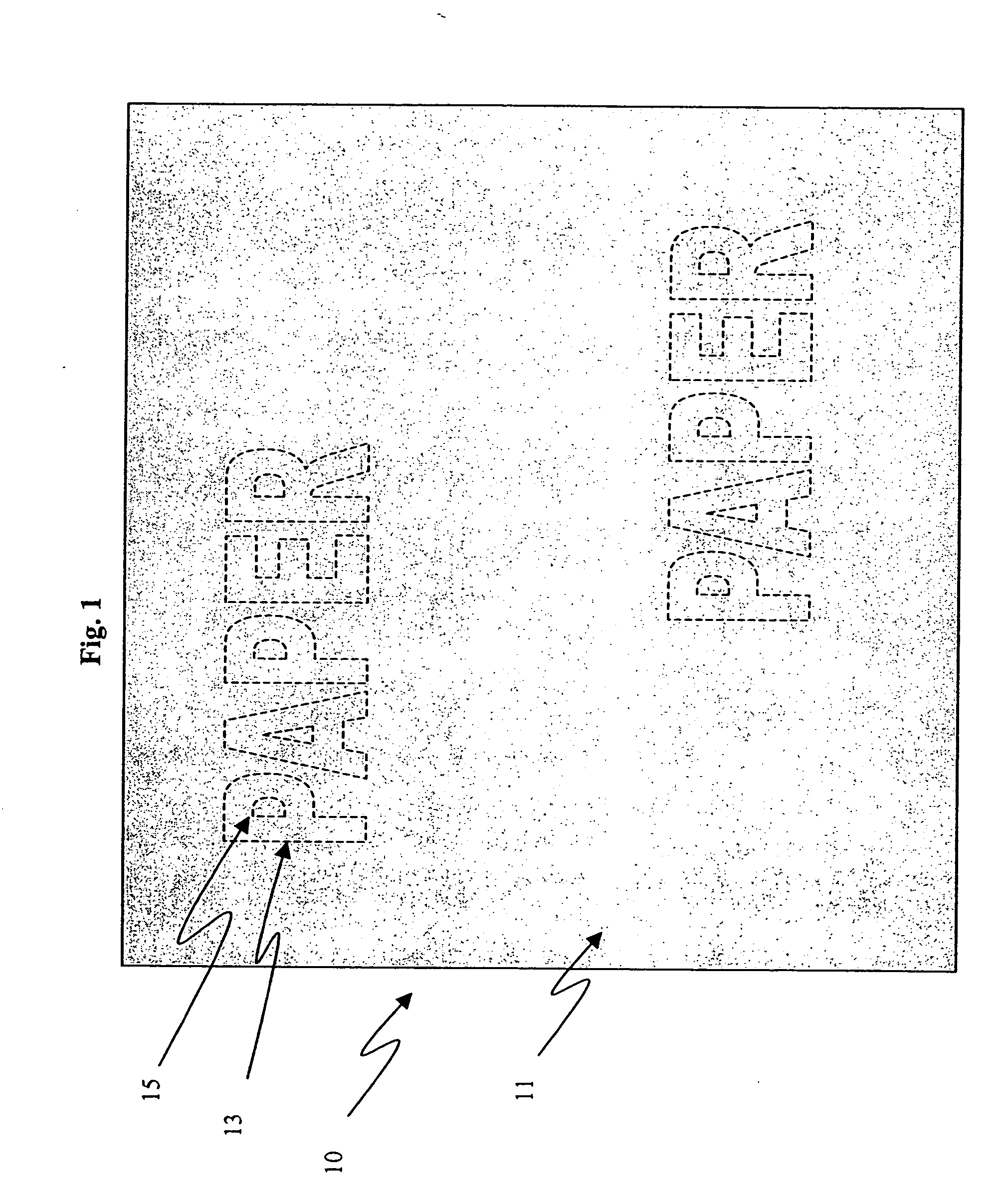
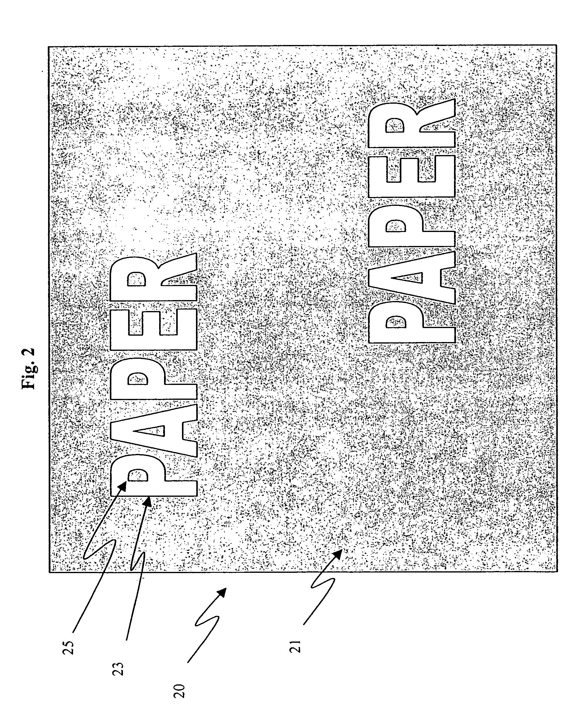
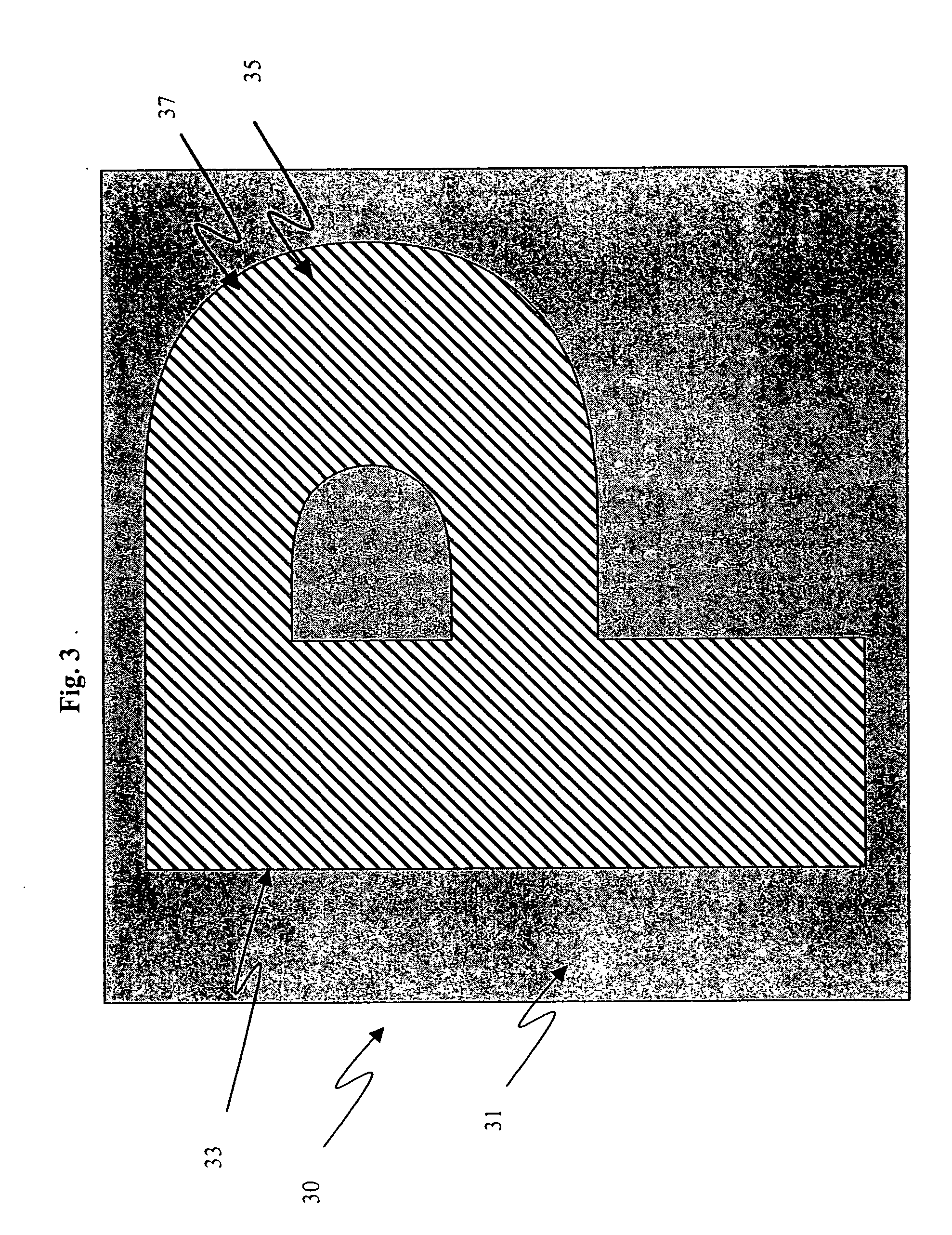
This example was prepared the same as example 1, except the antistatic layer was printed to form multiple logo graphics, with conductive lines between letters of the individual graphic design logos and also between each individual logo, as to form an interconnected pattern or grid as shown in FIG. 4.

TABLE 1Antistatic Layer CoatingExampleTypeSurface resistivity1 (control)Continuous3 × 109 ohms / sq.2Patterned grid with3 × 109 ohms / sq.internal logo

As shown by the data in Table 1, both the control, as represented by example 1, and the patterned grid with internal graphic design logo had the same level of surface resistivity.

Surface electrical resistivity (SER) is measured with a Keithly model 616 digital electrometer using a two point DC probe by a method similar to that described in U.S. Pat. No. 2,801,191, col.4, line 4-34. Internal resistivity or “water electrode resistivity (WER)” is measured by the procedures described in R. A. Elder, “Resistivity Measurement on Buried Conduct...


PUM

PropertyMeasurementUnit
Fractionaaaaaaaaaa
Percent by massaaaaaaaaaa
Weightaaaaaaaaaa

Abstract

The present invention relates to an article comprising a substrate having thereon at least one antistatic layer, wherein said antistatic layer comprises at least one conductive material, and wherein said antistatic layer comprises areas of patterned coverage, and wherein said patterned coverage comprises a graphic design.

Description

FIELD OF THE INVENTION The present invention relates to an antistatic layer having areas of patterned coverage in the form of a graphic design, such as a logo, applied to a support or a substrate. BACKGROUND OF THE INVENTION The problem of controlling static charge during plastic web manufacturing and transport is well known. Generation and uncontrolled discharge of electrostatic charge can cause a number of serious problems including safety hazards. In the field of imaging, particularly photography, the accumulation of charge on film or paper surfaces leads to the attraction of dirt, which can produce physical defects. The discharge of accumulated charge during or after the application of the sensitized emulsion layer(s) can produce irregular fog patterns or “static marks” in the emulsion. The static problems have been aggravated by increase in the sensitivity of new emulsions, increase in coating machine speeds, and increase in post-coating drying efficiency. The charge generate...

Claims


Application Information

Patent Timeline
IPC IPC(8): B32B3/00B41M5/00B41M5/40B41M5/41B41M5/50G03C1/74G03C1/85G03C1/89G03F7/00G03F7/09G03G7/00
CPCB41M5/41B41M5/506G03C1/74G03C1/85G03C1/895Y10T428/24802G03F7/093G03G7/0006G03G7/0046Y10T428/24612G03F7/002Y10T428/31855
Inventor AYLWARD, PETER T.MAJUMDAR, DEBASISFITZGERALD, BARRY A.ROBINSON, KELLY S.
Owner EASTMAN KODAK CO
Why Eureka
Try Eureka