Display panel and method for manufacturing the same

a display panel and manufacturing method technology, applied in the direction of manufacturing tools, identification means, instruments, etc., can solve the problems of deteriorating manufacturing yield and no thin film transistors in the region, and achieve high yield rate, high yield rate, and satisfying performance

Active Publication Date: 2005-03-31
PANASONIC LIQUID CRYSTAL DISPLAY CO LTD +1
View PDF4 Cites 34 Cited by
  • Summary
  • Abstract
  • Description
  • Claims
  • Application Information

AI Technical Summary

Benefits of technology

[0015] According to the method for manufacturing a display panel according to the present invention, a CW solid-state laser beam temporally modulated, that is, modulated in intensity of the laser beam in accordance with time, is condensed linearly on an amorphous silicon film formed on an insulating substrate of glass or the like. Thus, the amorphous silicon film is annealed and transformed to have performance satisfying performance required for a silicon film forming thin film transistors for use in each region including a region where thin film switching transistors forming a pixel portion should be formed, a region where a peripheral circuit including driver circuits should be formed, and so on. As a result, damage (occurrence of cohesion) on the silicon film is suppressed, or occurring damage (coherent portion) is prevented from extending to a broad range, so that display panels can be manufactured at a high yield rate. In addition, any annealing like this can be performed using a solid-state laser beam as a heat source. Thus, it is possible to reduce the running cost which has been required for performing excimer laser annealing in the background art.

Problems solved by technology

It has been, however, revealed experimentally that the aforementioned method has the following problem.
Therefore, no thin film transistor can be formed in the region.
A panel having such a coherent region becomes defective, so that the manufacturing yield deteriorates.

Method used


Image

  • Display panel and method for manufacturing the same
  • Display panel and method for manufacturing the same
  • Display panel and method for manufacturing the same

Examples


embodiment 1

[0050] Embodiment 1

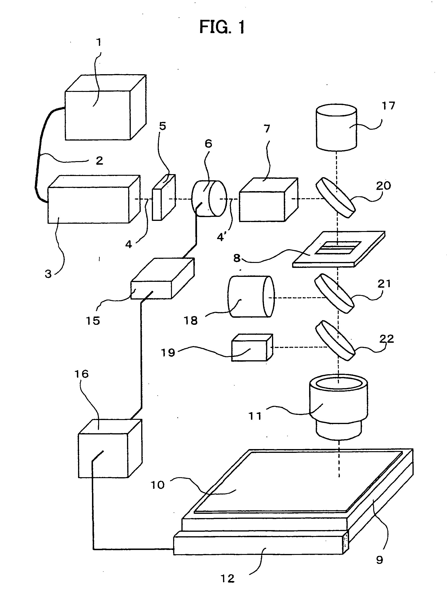
[0051]FIG. 1 is a schematic view for explaining a configuration example of an optical system and a control system of a laser annealing apparatus suitable for carrying out a method for manufacturing a display panel according to the present invention. In this configuration example, an LD pumped continuous-wave solid-state laser 3 by which infrared light generated from a laser (LD) placed in a laser power supply 1 is guided into an oscillator through an optical fiber 2 and excited in the oscillator is used as a laser source. The output of a continuous-wave (CW) laser beam 4 oscillated in the LD pumped continuous-wave solid-state laser (hereinafter referred to as “laser oscillator” simply) 3 is adjusted by an ND filter 5. The CW laser beam 4 is then incident on an EO modulator 6 so as to be temporally modulated by the EO modulator 6. The laser beam outputted from the EO modulator 6 passes through a homogenizer 7 for shaping the laser beam into a linear beam having an ...

embodiment 2

[0106] Embodiment 2

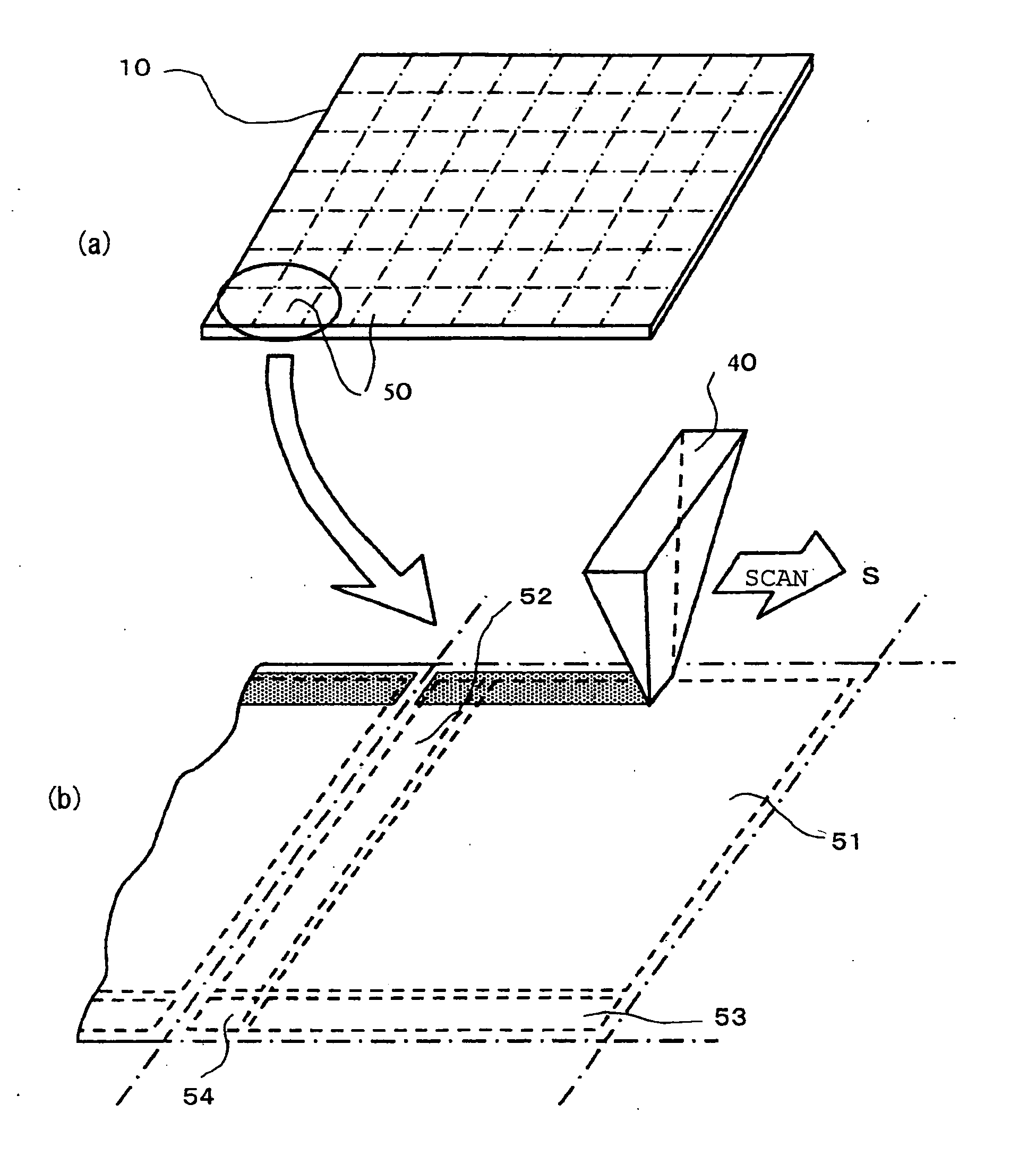
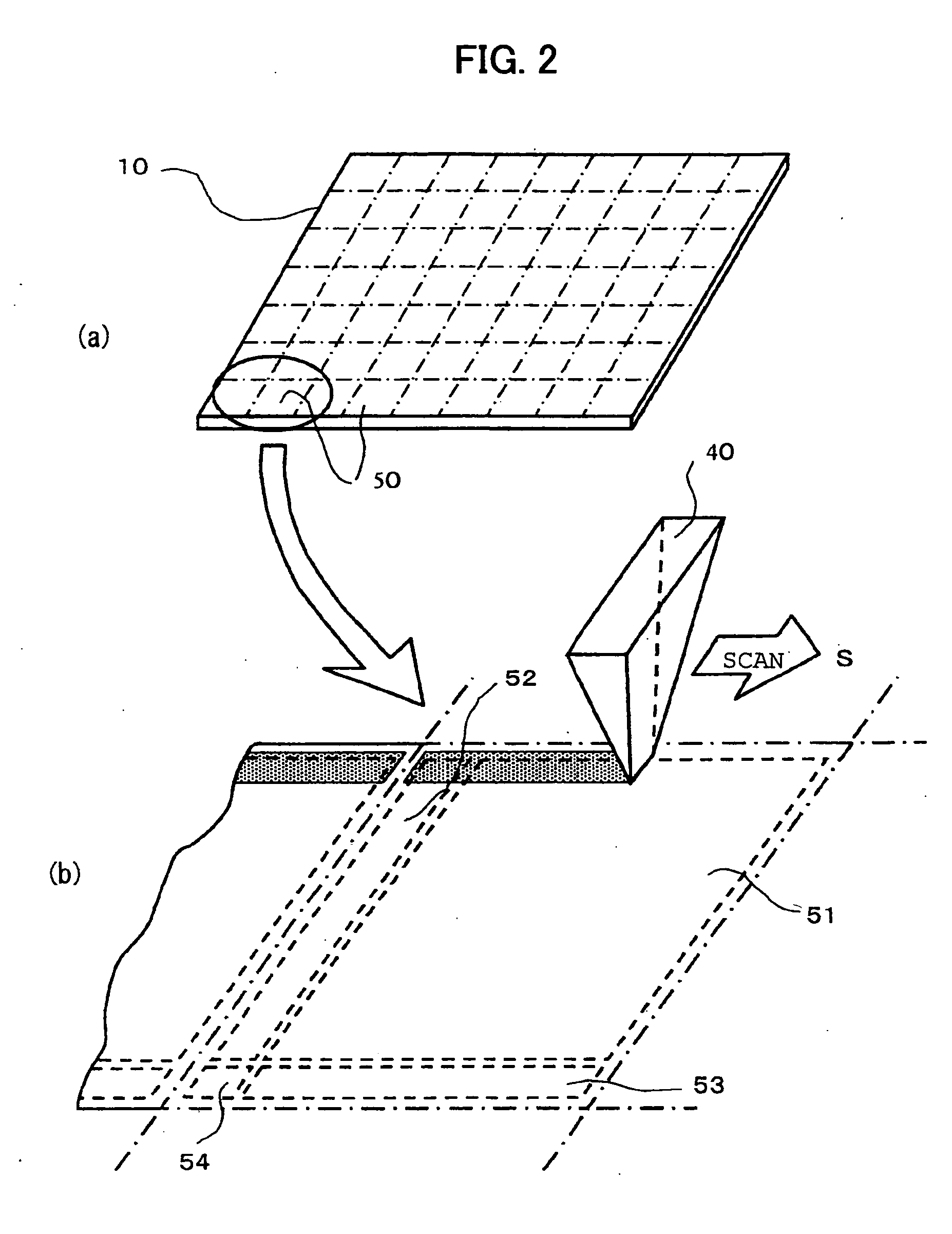
[0107]FIGS. 12A-12C are explanatory views showing the relationship between the stage movement and the power density of a laser beam for irradiation, for explaining Embodiment 2 of a method for manufacturing a display panel according to the present invention. See FIGS. 1 and 6 also for this description. In FIG. 12A, of a plurality of panels (typically several tens to several hundreds of panels are formed) to be formed out of a large-sized glass substrate, two panels adjacent to each other are shown representatively in the same manner as in Embodiment 1. Incidentally, an insulating substrate (glass substrate) forming each display panel will be referred to as “panel” here in the same manner as in Embodiment 1. A display portion (pixel portion) 181 (181′), a gate driver circuit portion 182 (182′), a drain driver circuit portion 183 (183′) and an additional peripheral circuit portion 184 (184′) are formed on each panel.

[0108] In this embodiment, a fine grain poly-crys...

embodiment 3

[0118] Embodiment 3

[0119]FIGS. 13A-13C are explanatory views showing the relationship between the stage movement and the power density of a laser beam for irradiation, for explaining Embodiment 3 of a method for manufacturing a display panel according to the present invention. See FIGS. 1 and 6 also for this description. In FIGS. 13A-13C, of a plurality of panels (typically several tens to several hundreds of panels are formed) to be formed out of a large-sized glass substrate, two panels adjacent to each other are shown representatively in the same manner as in Embodiment 2. The meaning of the word “panel” is similar to that in the aforementioned embodiments. In FIG. 13A, a display portion (pixel portion) 191 (191′), a gate driver circuit portion 192 (192′), a drain driver circuit portion 193 (193′) and an additional peripheral circuit portion 194 (194′) are formed on each panel.

[0120] In this embodiment, a fine grain poly-crystalline film unnecessary to be driven at a high speed ...


PUM

PropertyMeasurementUnit
surface roughnessaaaaaaaaaa
wavelengthaaaaaaaaaa
diameteraaaaaaaaaa

Abstract

An amorphous silicon film on an insulating substrate portion to be formed as an individual display panel in a large-sized insulating substrate is irradiated with a continuous-wave (CW) solid-state laser beam condensed linearly, while being scanned therewith at a fixed speed in the width direction of the condensed laser beam. A pixel portion and a peripheral circuit portion in the same insulating substrate portion are irradiated with the laser beam temporally modulated to have a power density high enough to provide predetermined crystallinity. The amorphous silicon film is transformed into a silicon film having crystallinity corresponding to performance required for thin film transistors to be built in each of the pixel portion and the peripheral circuit portion. In such a manner, a thin film transistor circuit having optimum crystallinity required in the pixel or peripheral circuit portion can be obtained while high throughput is kept. Thus, a product having good display features as a display panel can be provided inexpensively.

Description

BACKGROUND OF THE INVENTION [0001] The present invention relates to a method for manufacturing a display panel in which an amorphous or poly-crystalline semiconductor film formed on an insulating substrate is irradiated with a laser beam so that the film quality is improved or crystal grains are enlarged or transformed to be single-crystalline, and a display panel manufactured in the same manufacturing method, and particularly relates to a method for manufacturing a display panel having active devices such as thin film transistors formed out of a semiconductor film transformed to be single-crystalline, and a display panel manufactured in the same manufacturing method. [0002] In current liquid crystal or organic electroluminescence display units, an image is formed by switching thin film transistors formed out of an amorphous silicon film in a pixel portion (display region) on an insulating substrate of glass, fused quartz or the like. Exponential reduction in manufacturing cost and ...

Claims


Application Information

Patent Timeline
Patent Type & Authority Applications(United States)
IPC IPC(8): G02F1/1368B23K26/073G09F9/30H01L21/20H01L21/336H01L21/77H01L21/84H01L27/12H01L29/04H01L29/786
CPCB23K26/032B23K26/0639B23K26/0648B23K26/0652B23K26/0656B23K26/0665H01L29/78675H01L21/2026H01L27/1229H01L27/1285H01L27/1296H01L29/04H01L29/66757B23K26/0732B23K26/064B23K26/066H01L21/02683H01L21/02686H01L21/02678H01L21/02422H01L21/02532H01L21/02595H01L21/02691G02F1/1368
Inventor YAZAKI, AKIOHONGO, MIKIOHATANO, MUTSUKOSAITO, HIROSHIOHKURA, MAKOTO
Owner PANASONIC LIQUID CRYSTAL DISPLAY CO LTD
Why Eureka
Try Eureka