Organic thin film transistor enhanced in charge carrier mobility by virtue of surface relief structure

a thin film transistor and surface relief technology, applied in transistors, solid-state devices, thermoelectric devices, etc., can solve the problems of reducing charge carrier mobility, and inferiority of organic insulating layers

Inactive Publication Date: 2005-04-14
SAMSUNG ELECTRONICS CO LTD
View PDF6 Cites 6 Cited by
  • Summary
  • Abstract
  • Description
  • Claims
  • Application Information

AI Technical Summary

Benefits of technology

A feature of the present invention is to provide an organic TFT that has improved electronic properties, particularly charge carrier mobility, by forming a relief structure at the interface between an organic insulating layer and an organic active layer thereof.
In accordance with another feature of the present invention, there is provided a process of forming an organic insulating layer, wherein the process comprises the steps of: forming a film of an organic insulating polymer; and exposing the film to incident light from at least one light source of a particular wavelength in an interference pattern of a certain period, thereby making a difference of geometrical height between portions exposed to constructive interference and portions exposed to destructive interference to afford an organic insulating layer of desired surface relief structure.

Problems solved by technology

On the other hand, the use of organic materials such as polyimide, BCB(benzocyclobutene) and photoacryl in insulating layers of organic TFTs has been attempted, but such organic insulating layers were found inferior to inorganic insulating layers.
In these cases, however, the ceramic particles can affect the formation of an organic active layer and thereby decrease charge carrier mobility, or increase leakage current, resulting in using additional organic insulating materials.

Method used


Image

  • Organic thin film transistor enhanced in charge carrier mobility by virtue of surface relief structure
  • Organic thin film transistor enhanced in charge carrier mobility by virtue of surface relief structure
  • Organic thin film transistor enhanced in charge carrier mobility by virtue of surface relief structure

Examples


example 1

Formation of an Organic Insulating Layer of Surface Relief Structure

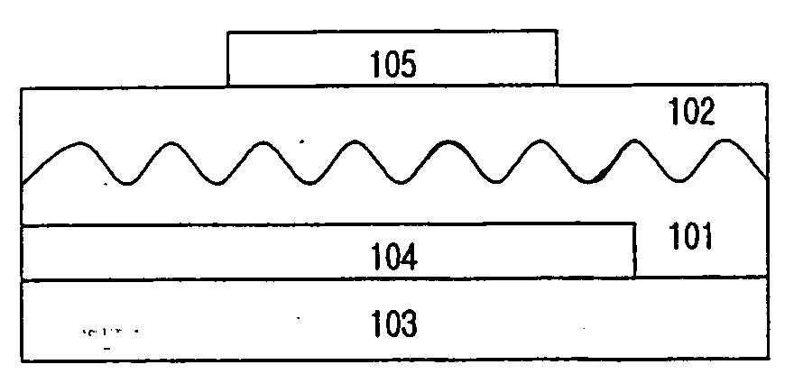
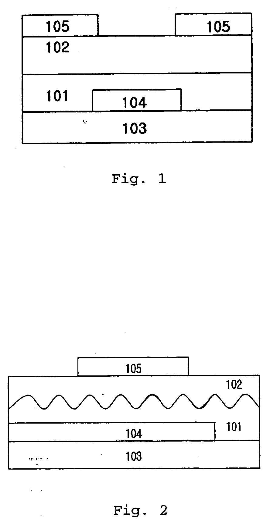
Onto a silicon substrate where a gate electrode was previously deposited, a 10 wt % solution of poly(4-nitrophenylazophenyloxylpentyl methacrylate-co-hydroxyethyl methacrylate) (Mw=35,000, MWD=2.5) in cyclohexanone was applied by spin coating to a thickness of 500 nm. The solvent was evaporated by drying the coated substrate at 100 □ for 10 minutes. The dried substrate was exposed to light having a wavelength of 488 nm by the use of a laser interferometer with an Ar+ laser. The incident angle of the laser beam was adjusted to 50° to afford a mono-axial lattice pattern having an interval period(Λ) of 500 nm and a depth of 50 nm. FIGS. 4a and 4b show AFM images of the resulting organic insulating layer.

example 2

Fabrication of an Organic TFT Device Using an Organic Insulating Layer of Surface Relief Structure

Onto the organic insulating layer of surface relief structure obtained from Example 1, a 1 wt % solution of poly(dioctylfulorene-co-bithiophene) in toluene was applied by spin coating to a thickness of 70 nm. The solvent was evaporated by drying the coated substrate at 100 □ for 30 minutes. On the resulting organic active layer were deposited source / drain electrodes by the use of a shadow mask having a channel length of 100 μm and a channel width of 2 mm to afford an organic TFT device. The direction of the channel length was equal to that of the major axis of the surface relief structure of the organic insulating layer.

example 3

Variation of the Electronic Properties of the Organic TFT Devices According to the Direction of the Surface Relief Structure

Two organic TFT devices, in which the major axis of the surface relief structure and the S-D channel were arrayed in the direction as shown in FIGS. 5a and 5b, were fabricated according to Examples 1 and 2 above. The current-transfer curves and charge carrier mobility curves of these devices were plotted in FIGS. 6 and 7, respectively. As a control, the current-transfer curve and charge carrier mobility curve of the device fabricated in the above Comparative Example were plotted simultaneously therewith.

As can be seen from FIGS. 6 and 7, device (II), in which the major axis of the surface relief structure and the S-D channel are parallel to each other, exhibited superior charge carrier mobility to the device (I), in which the major axis of the surface relief structure and the S-D channel are perpendicular to each other. On the other hand, device (I) exhibit...


PUM

PropertyMeasurementUnit
threshold voltageaaaaaaaaaa
dielectric constantaaaaaaaaaa

Abstract

Disclosed herein is an organic thin film transistor comprising a substrate, a gate electrode, an organic insulating layer, an organic active layer and source / drain electrodes, wherein the interface between the organic insulating layer and the organic active layer is of relief structure. According to the present invention, an organic thin film transistor of enhanced electric properties can be obtained regardless of the organic insulating materials used.

Description

BACKGROUND OF THE INVENTION This non-provisional application claims priority under 35 U.S.C. § 119(a) to Korean Patent Application No. 2003-70549 filed on Oct. 10, 2003, which is herein incorporated by reference. 1. Field of the Invention The present invention relates to an organic thin film transistor enhanced in charge carrier mobility by virtue of surface relief structure, and more particularly to an organic thin film transistor comprising a substrate, a gate electrode, an organic insulating layer, an organic active layer and source / drain electrodes, wherein the interface between the organic insulating layer and the organic active layer is of relief structure. 2. Description of the Related Art Recently, in the fields of functional electronic and optical elements, the use of polymers as new electronic materials has been actively researched. This is for several reasons, including their ease of molding, softness, conductivity and low production cost. Among those elements produc...

Claims


Application Information

Patent Timeline
Patent Type & Authority Applications(United States)
IPC IPC(8): H01L21/314H01L21/336H01L27/01H01L29/04H01L21/312H01L29/08H01L29/786H01L31/0392H01L51/00H01L51/05H01L51/30H01L51/40
CPCH01L21/312H01L51/00H01L51/0002H01L51/0545H01L51/0039H01L51/0043H01L51/0516H01L51/0036H01L21/02118H01L21/02282H10K71/10H10K99/00H10K85/115H10K85/151H10K85/113H10K10/468H10K10/466H01L29/786
Inventor SHIN, JUNG HANSEO, EUN MIHAN, KOOK MINBARMATOV, EVGENYSHIBAEV, VALERY
Owner SAMSUNG ELECTRONICS CO LTD
Why Eureka
Try Eureka