Microprobe for testing electronic device and manufacturing method thereof

a microprobe and electronic device technology, applied in the direction of measurement devices, semiconductor/solid-state device testing/measurement, instruments, etc., can solve the problems of large cost, long time and cost to test the wafer, and poor mechanical properties, so as to improve the mechanical and electrical properties improve the flatness of the probe tip, and reduce the time and cost of probing

Inactive Publication Date: 2005-05-05
SEOUL NAT UNIV R&DB FOUND
View PDF8 Cites 27 Cited by
  • Summary
  • Abstract
  • Description
  • Claims
  • Application Information

AI Technical Summary

Benefits of technology

[0015] Another object of the present invention is to improve flatness of a probe tip.
[0016] Another object of the present invention is to i...

Problems solved by technology

Further, all chips of the wafer can not be subject to simultaneous test and the chips should be tested in several times, so that it takes long time and big cost to test the wafer.
However, the probe card of FIG. 2 has a drawback in that it is susceptible to an external mechanical shock or temperature since a tip portion of the probe pattern 25 is formed with the solder ball 27.
However, the probe card of FIG. 3 has a drawback in that mechanical properties are bad since a tip of the conductive line is made of tungsten, gold or aluminum instead of a metal needle type tip.
The probe card of FIGS. 4a, 4b and 4c has a drawback in that it is manufactured difficultly and production cost is high since the probe tip is formed by a bonding technology such as a soldering.
The probe card of FIG. 5 has a structure for increasing elasticity using the leaf porti...

Method used


Image

  • Microprobe for testing electronic device and manufacturing method thereof
  • Microprobe for testing electronic device and manufacturing method thereof
  • Microprobe for testing electronic device and manufacturing method thereof

Examples


Embodiment Construction

[0045] Hereinafter, a preferred embodiment of the present invention will be described with reference to the accompanying drawings. In the following description and drawings, the same reference numerals are used to designate the same or similar components, and so repetition of the description of the same or similar components will be omitted.

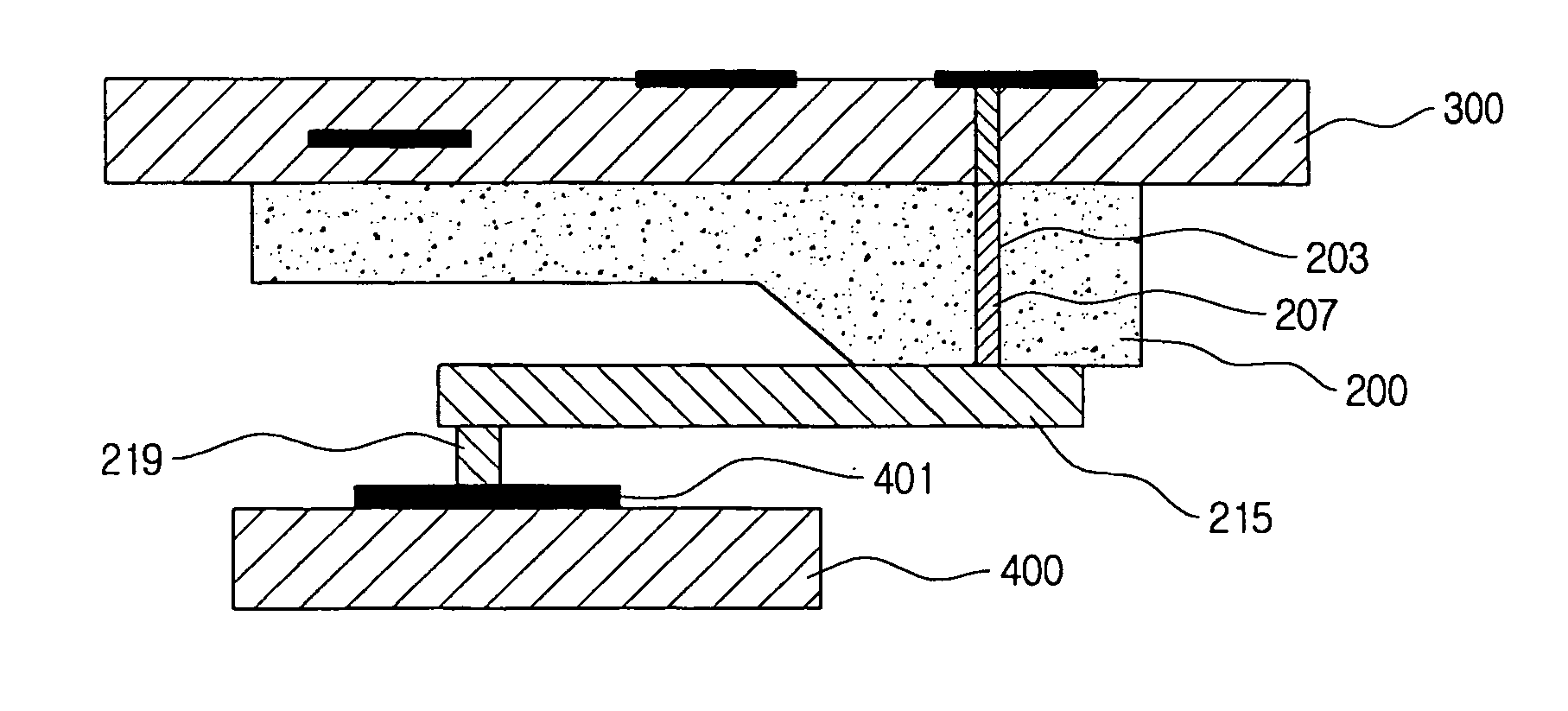
[0046] Referring to FIG. 8, a probe card using a microprobe of the present invention includes the microprobe and a printed circuit board 300. In the microprobe, a conductive layer 207 fills a via hole 203 formed on right edge portion of a single crystal silicon substrate 200. A conductive metal structured spring unit 215 is supported in a cantilever type on a bottom surface of right edge portion of the silicon substrate 200 and is electrically connected to the conductive layer 207. A conductive tip portion 219 to be in contact with a pad portion 401 of a wafer 400 is downwardly protruded from a leading end of the spring unit 215. An upper surfac...


PUM


Abstract

A microprobe is manufactured by forming via hole on one edge portion of the silicon substrate, filling the via hole with the conductive layer, forming the conductive spring unit on the silicon substrate so as to be electrically connected to the conductive layer in the via hole, forming the conductive tip portion on the leading end of the spring unit, removing the silicon substrate under the spring unit using isotropic etching, thereby supporting the spring unit only on the portion adjacent to the via hole. The spring unit and the tip portion are formed only in the window of a PR. The microprobe has benefits in that a separation of signal between tip portions is easy and mechanical and electrical properties of the probe tip are good, since the probe is formed on the silicon substrate by using micro-processing. Also, since the pitch between the tip portions can be reduced, a semiconductor device with fine pitch pad can be tested. Furthermore, the uniformity of flatness of the probe tip portion can be improved.

Description

BACKGROUND OF THE INVENTION [0001] 1. Field of the Invention [0002] The present invention relates to a microprobe for testing electrical characteristics of semiconductor devices, and more particularly to a microprobe for testing electrical characteristics of semiconductor devices and a manufacturing method thereof which reduces pitch of a probe tip and improves a flatness and a uniformity by forming a cantilever type probe on a silicon substrate using MicroElectroMechanical Systems (MEMS). [0003] 2. Description of the Related Art [0004] In a manufacturing process for semiconductor Integrated Circuit (IC) devices such as memory devices, non-memory devices or logic devices, after chips are fabricated on a wafer such as a silicon substrate, the wafer is tested to determine if an individual chip is good or defective before the chips of the wafer are cut into separate chips. The test is generally performed in a state that a probe card is connected to a probe device and a probe needle of ...

Claims


Application Information

Patent Timeline
IPC IPC(8): G01R1/067H01L21/66G01R1/073G01R3/00
CPCG01R1/06711G01R1/06727G01R3/00G01R1/07342G01R1/06744H01L22/00
Inventor CHUN, KUK JINKIM, BONG HWAN
Owner SEOUL NAT UNIV R&DB FOUND
Why Eureka
Try Eureka