Large-scale colloidal crystals and macroporous polymers and method for producing
a macroporous polymer and colloidal crystal technology, applied in the direction of silicon compounds, other chemical processes, instruments, etc., can solve the problems of destroying photonic band gaps, inability to scale up to industrial-scale mass production, and inability to control thickness
- Summary
- Abstract
- Description
- Claims
- Application Information
AI Technical Summary
Benefits of technology
Problems solved by technology
Method used
Image
Examples
example 1
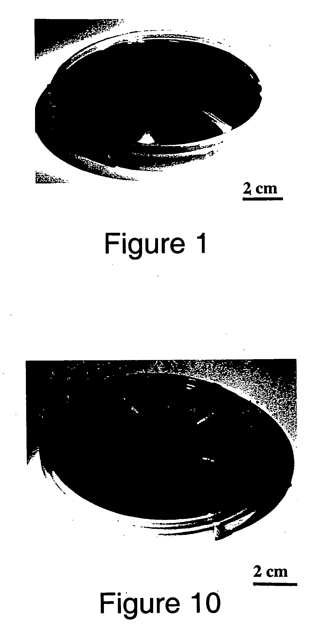
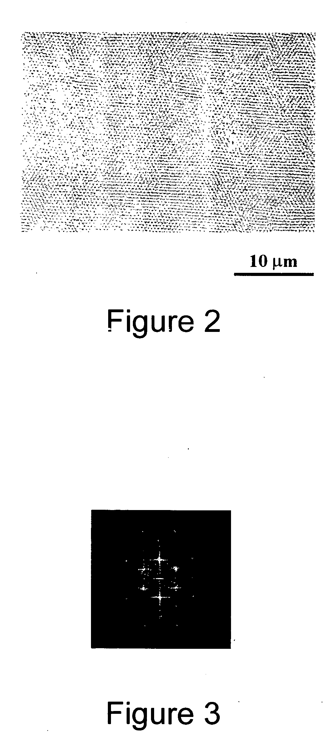
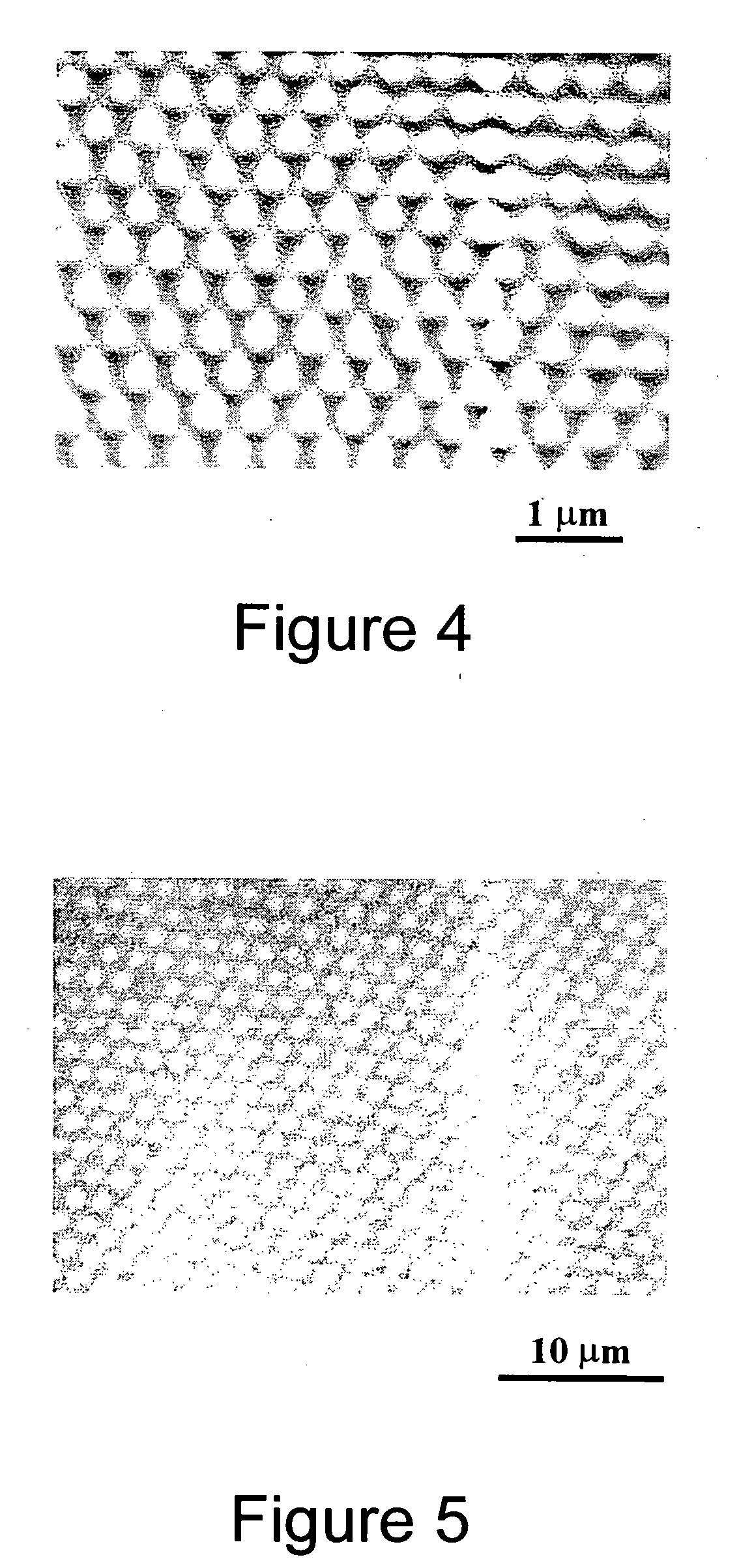
[0063] In accordance with the foregoing, four-inch silicon wafer was spin-coated with a colloidal suspension of 325 nm diameter spheres at 600 rpm for 120 seconds. The monomer was the polymerized as described above. FIGS. 1, 2, 4, and 6 show the resulting 41-layer nanocomposite film. A Nikon Optiphot 200C light microscope in confocal mode was used to optically section the nanocomposite film shown in FIG. 1. Each layer of the film exhibited hexagonal long-range ordering of spheres. A scanning electron microscope (SEM) image, FIG. 2, and its Fourier transform, FIG. 3, demonstrate the highly ordered structures with hexagonal packing on the film surface. At higher magnification, another interesting feature is evident, i.e. the spheres of the top layer are not touching each other, but exhibit center-to-center distance around 1.41 D (FIG. 3), where D is the diameter of colloids. This is possibly caused by spatial repulsion between colloidal spheres, arising from the adsorbed monomer layer...
example 2
[0064] A nanocomposite film was produced in accordance with the foregoing by spin-coating a dispersion of 1320 nm diameter spheres at 600 rpm for 120 seconds. The resulting nanocomposite film is shown in the SEM image of FIG. 5.
example 3
[0065] A nanocomposite film was produced in accordance with the foregoing by spin-coating a dispersion of 325 nm diameter spheres at 6000 rpm for 170 seconds. A side view image of the resulting 5-(five-) layer nanocomposite film is shown in FIG. 7. The same process, after removal of the polymer material, produced the 5-layer colloidal crystal on a 4-inch silicon wafer shown in FIGS. 10, 11, and 13.
PUM
| Property | Measurement | Unit |
|---|---|---|
| diameter | aaaaa | aaaaa |
| diameter | aaaaa | aaaaa |
| thickness | aaaaa | aaaaa |
Abstract
Description
Claims
Application Information


