Method of manufacturing semiconductor device

a manufacturing method and semiconductor technology, applied in the direction of semiconductor devices, basic electric elements, electrical appliances, etc., can solve the problems of increasing manufacturing costs, difficult to form contact between a junction area and a bit line, and difficulty in making a contact between upper and lower, so as to prevent process troubles in the manufacture

Inactive Publication Date: 2005-05-05
SK HYNIX INC
View PDF9 Cites 4 Cited by
  • Summary
  • Abstract
  • Description
  • Claims
  • Application Information

AI Technical Summary

Benefits of technology

[0011] Accordingly, the present invention has been made to solve the above-mentioned problems occurring in the prior art, and an object of the present invention is to provide a method of manufacturing a semiconductor device capable of preventing process troubles in the manufacture of semiconductor devices.

Problems solved by technology

As semiconductor devices have come highly integrated, there is difficulty in making a contact between upper and lower patterns, that is, it is difficult to form a contact between a junction area and a bit line and between a junction area and a capacitor.
However, such a conventional semiconductor manufacturing process may necessarily cause a step difference between a cell region and a peripheral region, so it is necessary to recess the cell region by performing a cell-open mask forming process and an etching process by using a cell-open mask in order to ensure reliability of the following processes.
Therefore, the conventional semiconductor manufacturing process not only causes some trouble in the manufacture of semiconductor devices, but also increases manufacturing costs.
For this reason, an oxide layer must be additionally deposited in order to solve the above dishing problem, thereby causing some trouble in the manufacture of semiconductor devices.
In this case, a bridge is created between bit line contacts or storage node contacts, thereby causing yield loss.

Method used


Image

  • Method of manufacturing semiconductor device
  • Method of manufacturing semiconductor device
  • Method of manufacturing semiconductor device

Examples


Embodiment Construction

[0020] Hereinafter, a preferred embodiment of the present invention will be described with reference to the accompanying drawings. In the following description and drawings, the same reference numerals are used to designate the same or similar components, and so repetition of the description on the same or similar components will be omitted.

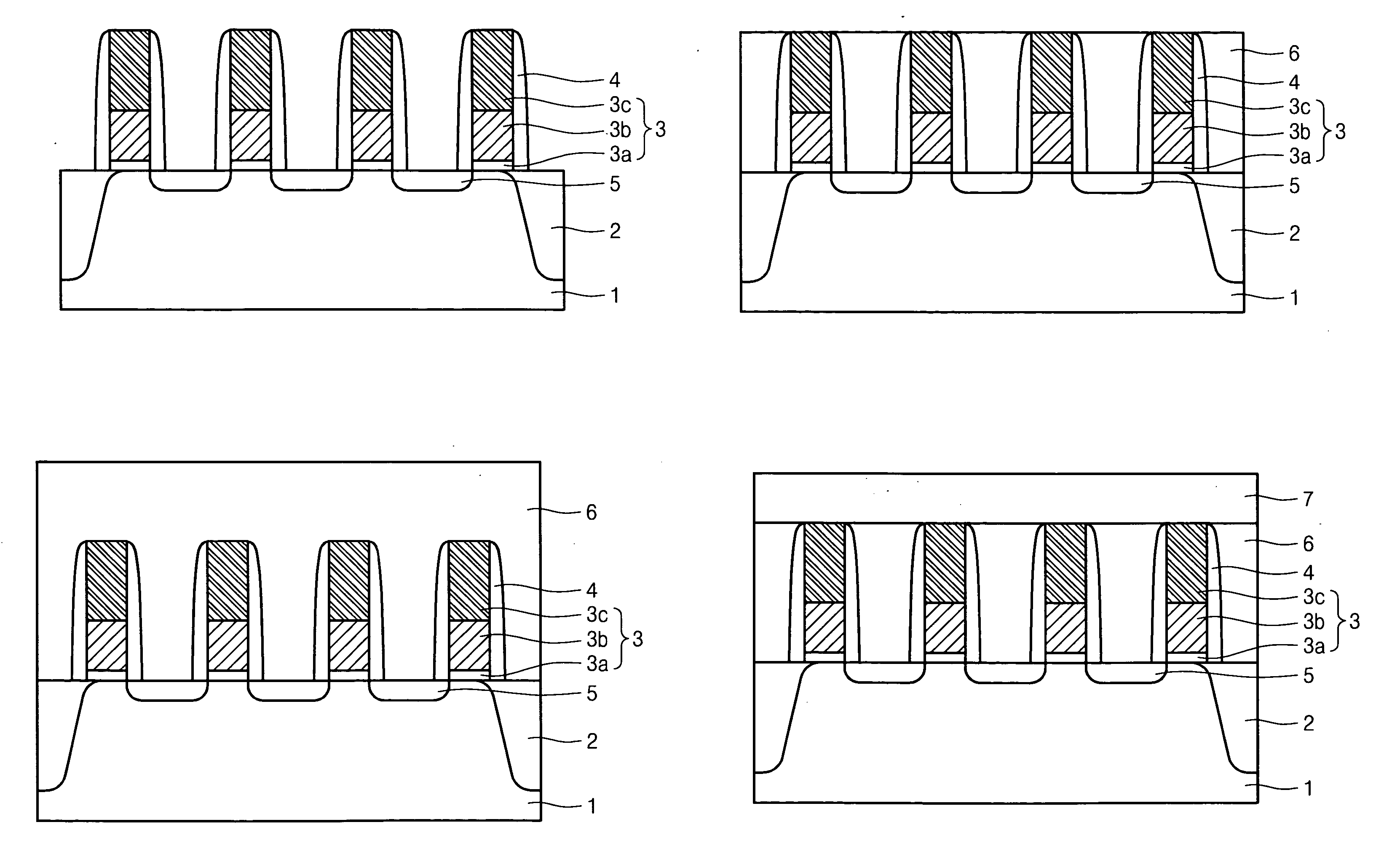
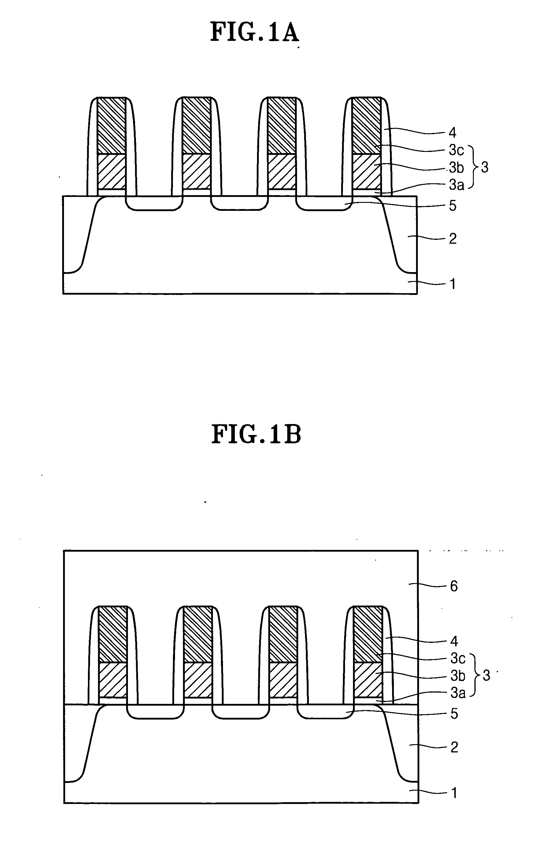
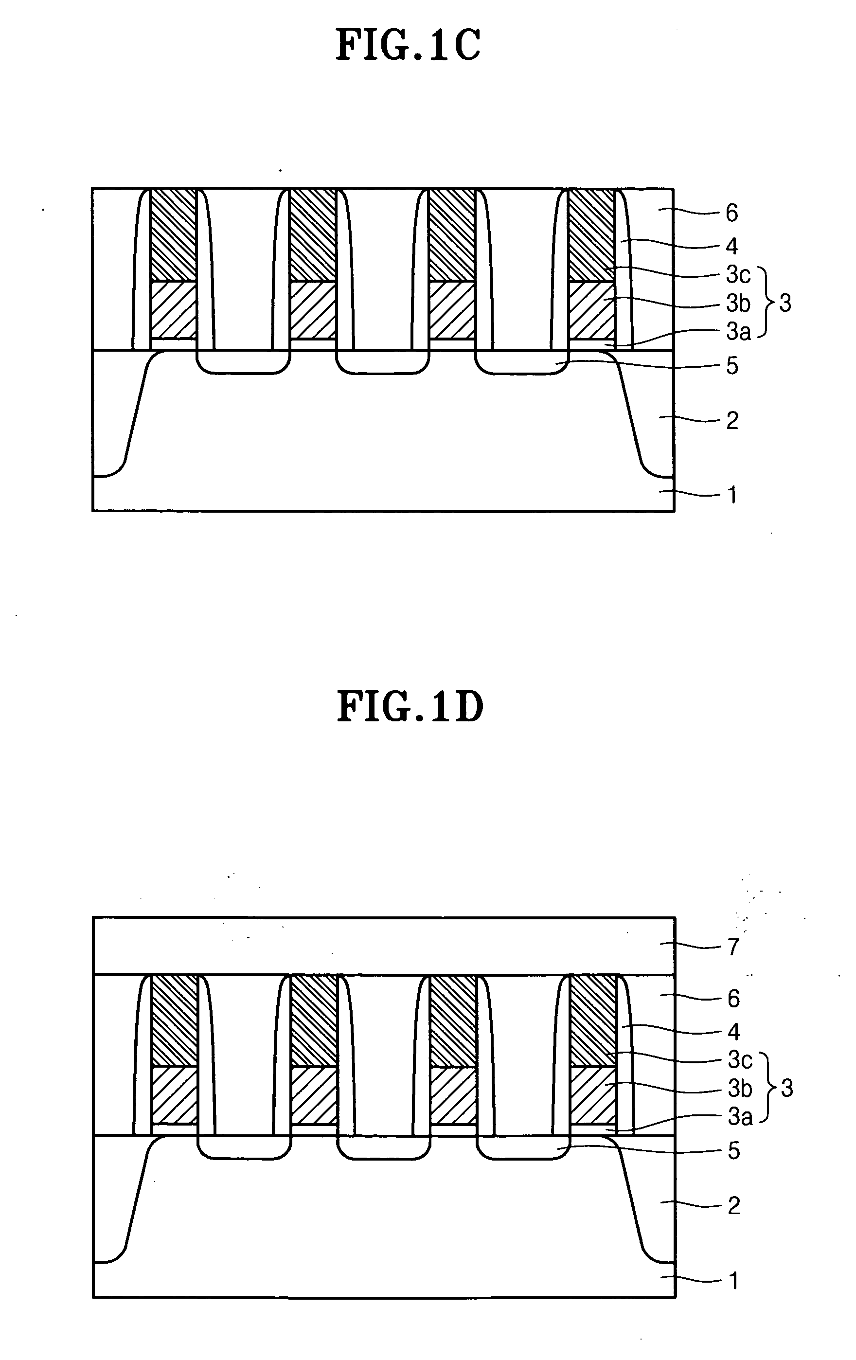
[0021]FIGS. 1a to 1g are sectional views for explaining a method of manufacturing a semiconductor device according to one embodiment of the present invention.

[0022] Referring to FIG. 1a, a semiconductor substrate 1 having trench-type isolation layers 12 formed through an STI (shallow trench isolation) process for defining an active area is prepared. Then, a gate oxide layer 3a, a gate conductive layer 3b in the form of a stacked layer of polysilicon and tungsten or tungsten silicide, and a nitride hard mask 3c are sequentially formed on the semiconductor substrate 1. After that, the nitride hard mask 3c, the gate conductive layer 3b, and the ga...


PUM


Abstract

Disclosed is a method of manufacturing a semiconductor device. The method includes the steps of forming gates on a substrate, forming junction areas on a surface of the substrate, forming a first BPSG layer on a resultant structure of the substrate, performing a first CVD process for the first BPSG layer, forming a second BPSG layer on the first BPSG layer, forming a landing plug contact, depositing a polysilicon layer on a resultant structure of the substrate, and performing a second CMP process for the polysilicon layer, the second BPSG layer and the nitride hard mask. The CMP processes are carried by using acid slurry having a high polishing selectivity with respect to the nitride layer, so a step difference between the cell region and the peripheral region is removed, thereby simplifying the semiconductor manufacturing process and removing a dishing phenomenon.

Description

BACKGROUND OF THE INVENTION [0001] 1. Field of the Invention [0002] The present invention relates to a method of manufacturing a semiconductor device, and more particularly to a method of manufacturing a semiconductor device capable of preventing process failure caused by a step difference between a cell region and a peripheral region and preventing yield loss derived from such process failure. [0003] 2. Description of the Prior Art [0004] As semiconductor devices have come highly integrated, there is difficulty in making a contact between upper and lower patterns, that is, it is difficult to form a contact between a junction area and a bit line and between a junction area and a capacitor. [0005] To solve the above problems, a landing plug poly is currently adopted in most of semiconductor manufacturing processes in order to form a stable electric contact between upper and lower patterns. Electric connection between the junction area and the bit line and between the junction area an...

Claims


Application Information

Patent Timeline
Patent Type & Authority Applications(United States)
IPC IPC(8): H01L21/304H01L21/44H01L21/4763H01L21/283H01L21/60H01L21/768H01L21/822H01L21/8242
CPCH01L21/7684H01L21/76897H01L27/10888H01L27/10873H01L27/10855H10B12/05H10B12/485H10B12/0335H01L21/283
Inventor LEE, SANG ICKSHIN, JONG HANPARK, HYUNG SOON
Owner SK HYNIX INC
Why Eureka
Try Eureka