

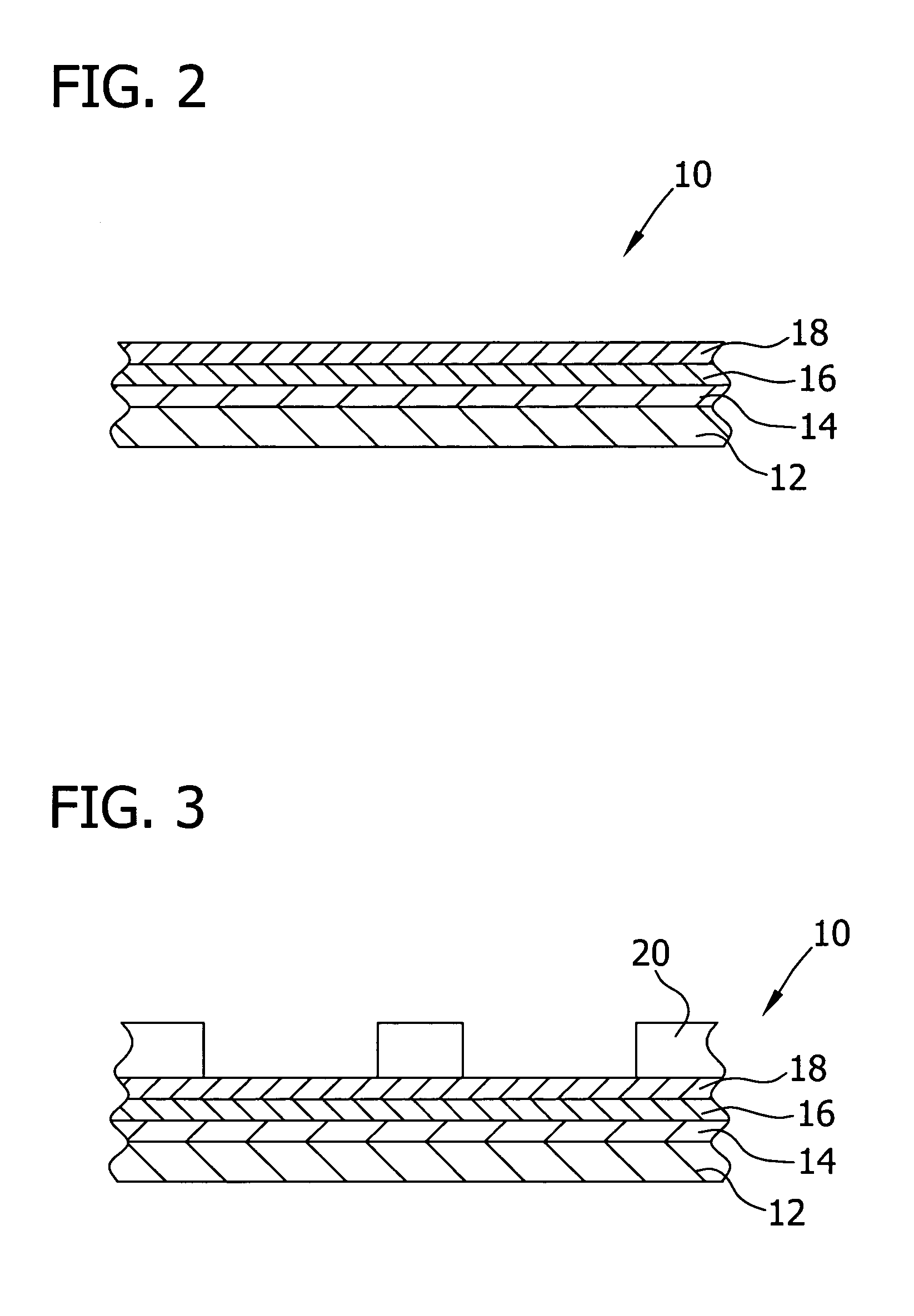
Deposition and patterning process
a patterning and deposition technology, applied in the field of deposition and patterning process, can solve the problems of cumbersome process of creating substrates with varying thicknesses, insufficient precision required to appropriately form desired patterns, etc., and achieve the effect of reducing or eliminating the edge effect and inhibiting the edge
- Summary
- Abstract
- Description
- Claims
- Application Information
AI Technical Summary
Benefits of technology
Problems solved by technology
Method used
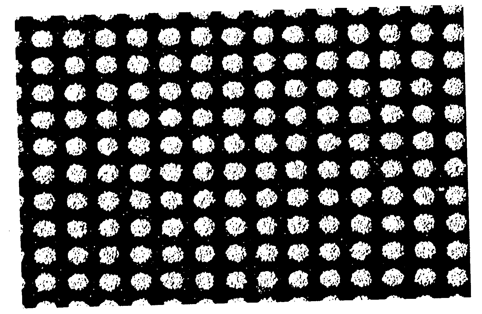
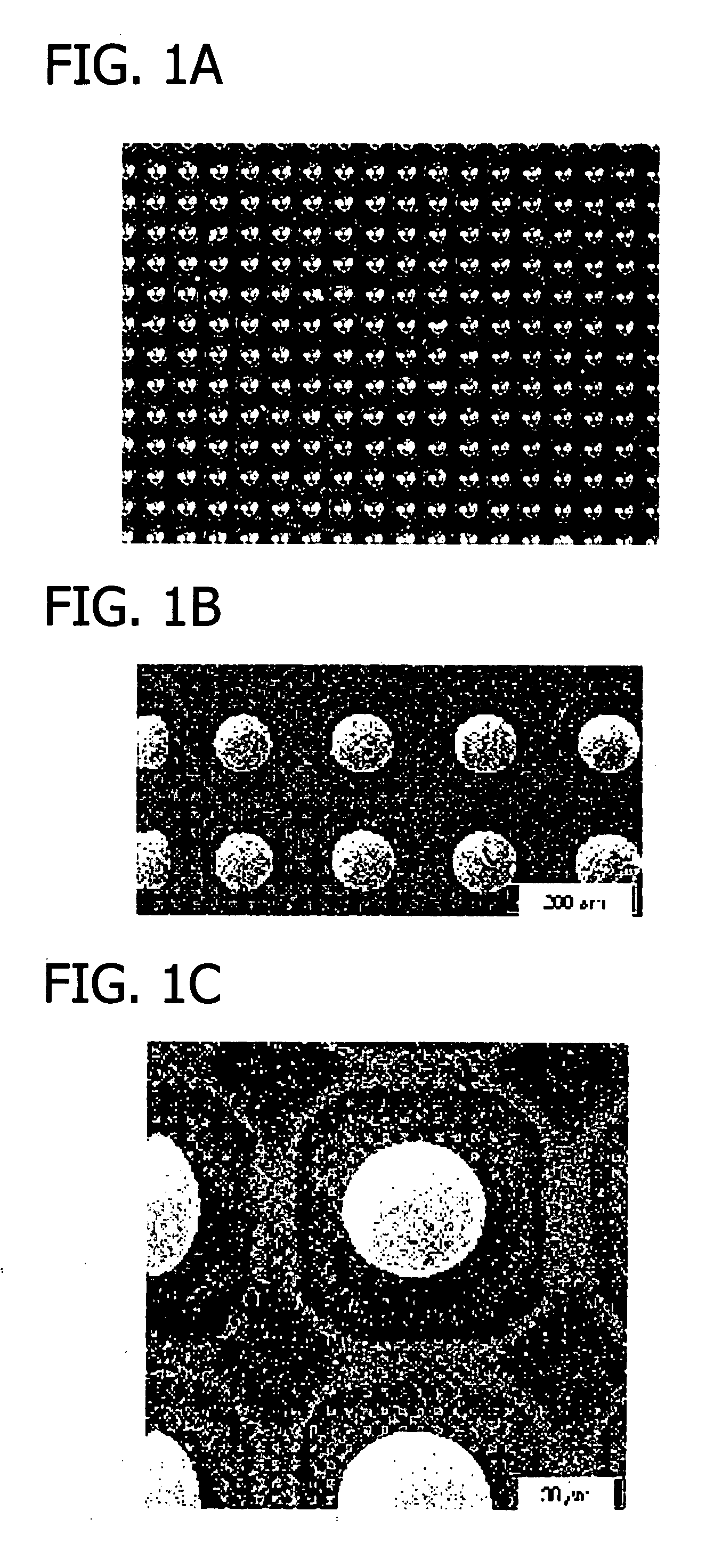
Image

Examples
example 1
[0081] For preparation of a charge director, barium petronate (10 g) available from Crompton Corporation of Middlebury, Conn. (USA) is added to Isopar G (90 g) available from ExxonMobil Chemical Company of Houston, Tex. (USA) in a 200 ml beaker. The beaker is placed on a heated stir plate and heated / stirred until it reaches a temperature of 80-90 C. Highly polished water (10 g), i.e., very pure distilled water is added one drop (˜16 micro-liter) at a time while the solution is continually stirred and heated. After all the water is added the solution is stirred and heated for a further one hour. The heat is then removed and stirring is continued until the solution has cooled. A tan-colored precipitate is noted to form. The mixture is aged for one day at room temperature, then filtered and the precipitate discarded.
example 2
[0082] For solder powder coating, Joncryl 682 resin available from Johnson Polymer, LLC of Studevant, Wis. (USA) is dissolved in methanol to a concentration of 20% then spray coated onto Type 6 Sn63Pb37 solder powder obtained from Welco GmbH, Potsdam, Germany. The spraying is achieved by a Wurster Process performed by Coating Place, Inc. of Verona, Wis. (USA).
example 3
[0083] For toner preparation, coated powder (120 g) is added to 1 liter of Isopar G in a 1.4 liter beaker and stirred with an appropriate mixer, such as “The Agitator” available from Victory Engineering, Hillside, N.J. (USA). Magnetic stir bars are not used because they abrade the coating off the powder. Charge director (21 drops; −0.016 ml per drop) prepared according to Example 1 is added to the mixture and the stirring continued for at least four hours. The toner is allowed to age for two days at room temperature. The toner is protected from a high humidity environment (>60% RH) to maintain stable performance.
PUM
| Property | Measurement | Unit |
|---|---|---|
| Diameter | aaaaa | aaaaa |
| Diameter | aaaaa | aaaaa |
| Diameter | aaaaa | aaaaa |
Abstract
Description
Claims
Application Information