
Formation method of metal layer on resin layer, printed wiring board, and production method thereof

a technology of resin layer and printing method, applied in the direction of resistive material coating, metal layered products, metallic material coating process, etc., can solve the problems of roughened shape, inverse interference with fine wiring formation, electric characteristics deterioration, etc., to suppress wiring dispersion and occurrence of defection, excellent electric properties

Inactive Publication Date: 2005-05-19
HITACHI CHEM CO LTD
View PDF11 Cites 32 Cited by
  • Summary
  • Abstract
  • Description
  • Claims
  • Application Information

AI Technical Summary

Benefits of technology

[0027] According to the above embodiments of the invention, there is no such a defect that gold plating is deposited on a resin, and fine wiring formation with accuracy is realized.
[0049] According to the above-mentioned embodiments, a wiring board advantageous in the fine wiring formation, electric properties, and production cost can be obtained and a wiring board excellent in high frequency properties can be obtained as well.
[0067] According to the embodiments, an inner conductor circuit treatment method capable of providing excellent electric properties and suppressing dispersion of wiring and occurrence of defection is provided.

Problems solved by technology

However, according to these methods, the roughened shape inversely interferes the fine wiring formation.
Moreover, the electric characteristics are deteriorated by the roughened shape.
However, the substrate is very expensive and thus does not become popular.
However, in the case of gold plating after the circuit formation, a trouble that the gold plating is deposited on the resin sometimes occurs at the time of electroless gold plating according to the above-mentioned method disclosed in JP-A No. 10-4254.
Especially, in the case the wiring pitches become 80 μm or narrower, the trouble occurs more frequently.
Also, in the case of gold plating after the circuit formation, a trouble that the gold plating is deposited on the resin sometimes occurs owing to remaining of a copper foil on the resin at the time of electroless gold plating according to the above-mentioned method disclosed in JP-A No. 2003-158364.
However, these methods tend to cause problems that the electric properties are deteriorated: that plating is deposited on the portion other than the conductor circuits along with the advanced fineness of the circuits: and that plating between fine circuits is insufficient.
Further, there occur problems that the resistance of the conductor is increased because of etching of the conductor circuit and the dispersion of the wiring becomes wide.

Method used


Image

  • Formation method of metal layer on resin layer, printed wiring board, and production method thereof
  • Formation method of metal layer on resin layer, printed wiring board, and production method thereof
  • Formation method of metal layer on resin layer, printed wiring board, and production method thereof

Examples


example 1a

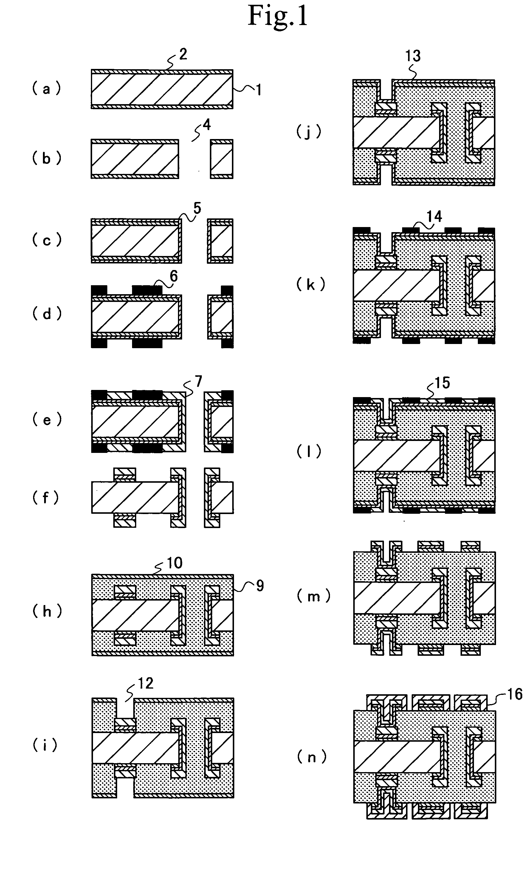
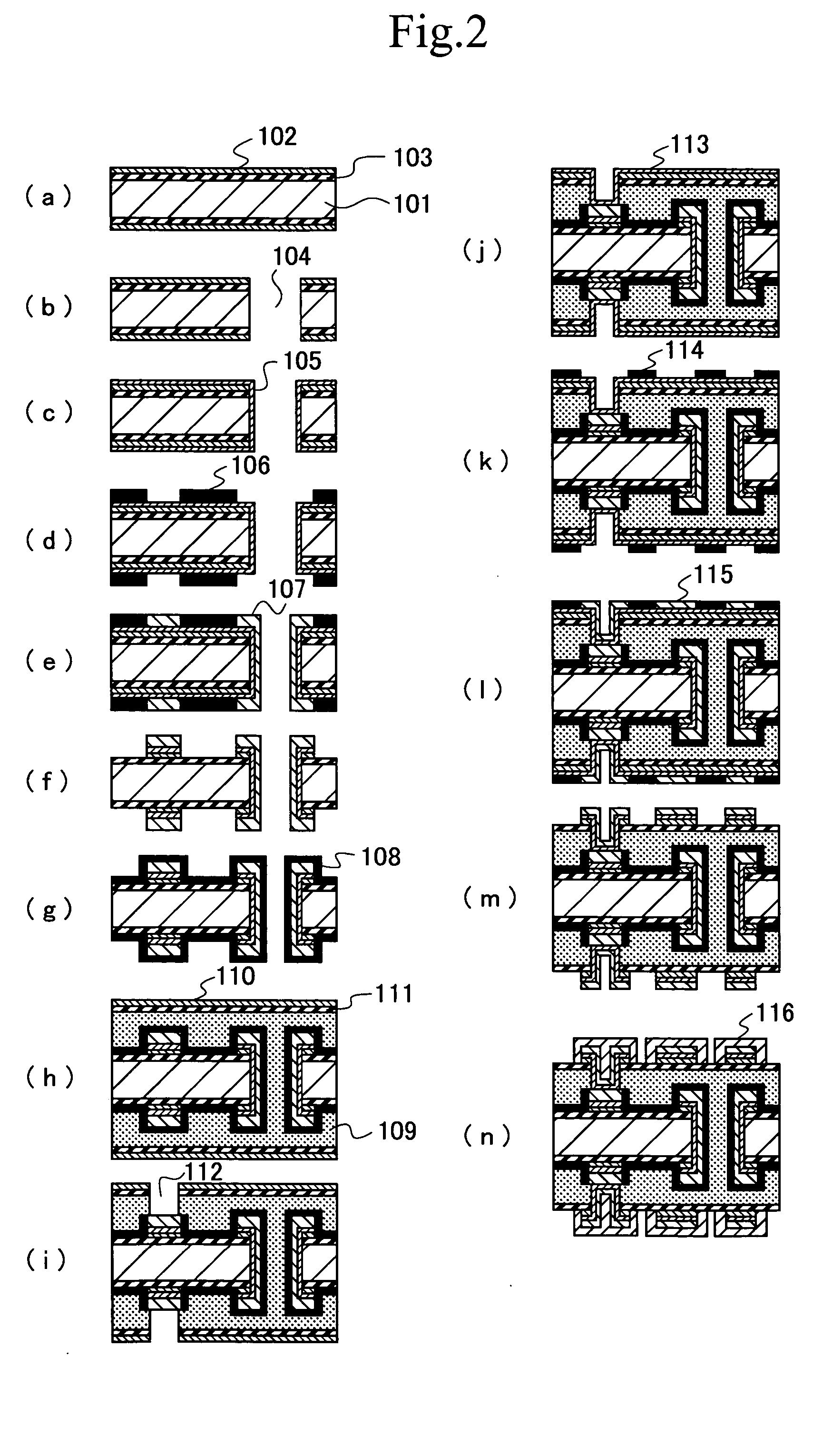
[0179] The following metal foil A was produced.

Metal Foil A

[0180] Chromium plating was continuously carried out on the bright face of an electrolytic copper foil (a carrier copper foil) with a width of 510 mm and a thickness of 35 μm in the following conditions to form a chromium plating layer (a separation layer) with a thickness of 1.0 mg / dm2. The surface roughness (ten-point mean surface roughness) Rz after the chromium plating formation was 0.5 μm. The surface roughness was measured according to JIS-B-0601.

[0181] Solution composition: chromium trioxide 250 g / L and sulfuric acid 2.5 g / L,

[0182] Bath temperature: 25° C.,

[0183] Anode: lead, and

[0184] Electric current density: 20 A / dm2.

[0185] Next, electric copper plating in a thickness of 2.0 μm was carried out in the following bright conditions. The metal foil surface roughness Rz after the electric copper plating was 0.6 μm.

[0186] Solution composition: copper sulfate pentahydrate 100 g / L, sulfuric acid 150 g / L, and chlori...

example 1b

[0222] The following resin composition A was produced.

Resin Composition A

[0223] A separable flask 500 mL capacity equipped with a Deen / Stark ref luxing cooling apparatus, a thermometer, and a stirrer was loaded with (4,4′-diamino)dicyclohexylmethane as an alicyclic diamine compound (trade name: Wondamine HM (abbreviated as WHM), manufactured by New Japan Chemical Co., Ltd.) 45 mmol, a reactive silicone oil X-22-161-B as siloxanediamine (trade name: manufactured by Shin-Etsu Chemical Co., Ltd., amine equivalent 1,500) 5 mmol, trimellitic anhydride (TMA) 105 mmol, and N-methyl-2-pyrrolidone as a non-proton polar solvent 145 g and the mixture was stirred at 80° C. for 30 minutes.

[0224] On completion of stirring, toluene 100 mL as an aromatic hydrocarbon azeotropic with water was added and the resulting reaction solution was heated to 160° C. and refluxed for 2 hours. When it was confirmed that a theoretical quantity of water was pooled in a water quantitative reception apparatus an...

example 2b

[0239] A substrate was produced in the same manner as Example 1B, except that GEA-679-FG, which is prepreg with 60 μm thickness and metal foils B were laminated on the inner substrate in place of application and heating of the resin composition B after the coating in the step G.


PUM

PropertyMeasurementUnit
Temperatureaaaaaaaaaa

Abstract

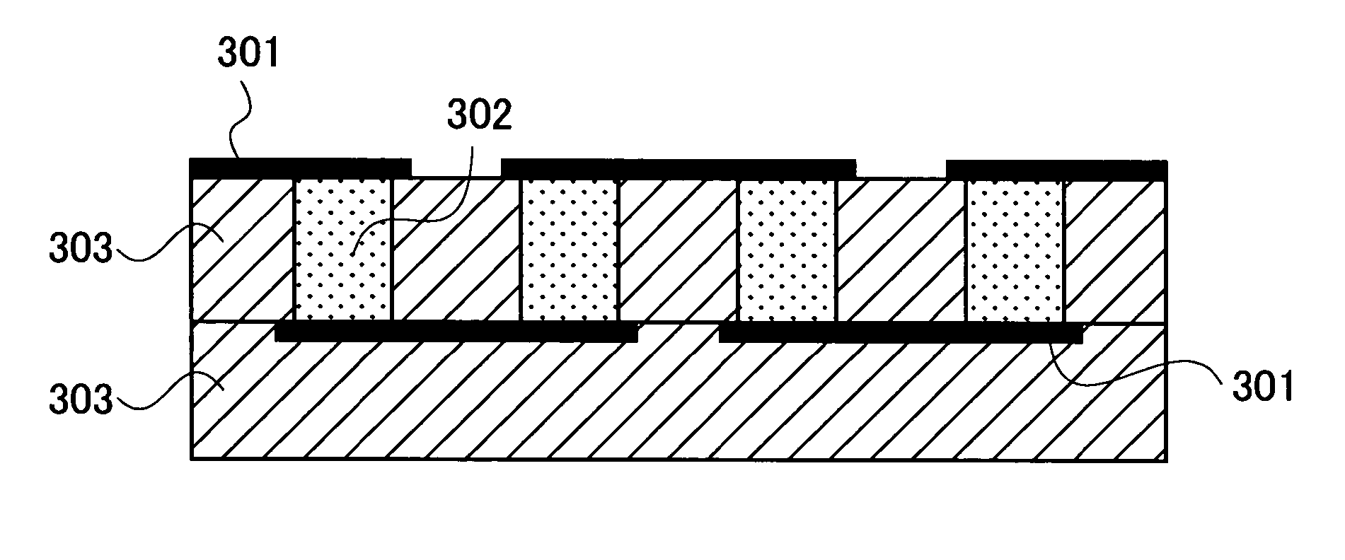
A printed wiring board having a conductor circuit comprising a copper layer adjacent to an insulating layer and an electroless gold plating, wherein the insulating layer has ten-point mean surface roughness (Rz) of 2.0 μm or less is provided. According to the present invention, there is no such a defect that gold plating is deposited on a resin, and fine wiring formation with accuracy is realized.

Description

BACKGROUND OF THE INVENTION [0001] 1. Field of the Invention [0002] The invention relates to a printed wiring board and its production method. Further, the invention relates to a formation method of a resin layer on a metal layer, an inner conductor circuit treatment method, and a multilayer circuit board. [0003] 2. Description of the Related Art [0004] Recently, electronic devices have been required to be compact, lightweight and high speed, and high densification of printed wiring boards has been advanced. Along with that, production of a printed wiring board by a semi-additive method using electroplating has been drawing an attention. As a semi-additive method, Japanese Patent Application Laid-Open No. 10-4254 discloses a method involving forming holds to be IVH in the resin surface in which a circuit is to be formed by laser; surface-roughening the resin surface with several μm by chemical roughening or plasma treatment; supplying a Pd catalyst; carrying out electroless plating ...

Claims


Application Information

Patent Timeline
IPC IPC(8): H05K3/18C23C18/12H05K3/10H05K3/24H05K3/38H05K3/46
CPCC23C18/1608Y10S428/901C23C18/2093C23C18/31C25D5/022H05K3/108H05K3/244H05K3/386H05K3/427H05K3/4644H05K3/4652H05K2201/0154H05K2201/0355H05K2203/072Y10T29/49124Y10T29/49126Y10T428/24917Y10T428/12472Y10T428/12514Y10T29/4913Y10T428/12493Y10T428/12535Y10T29/49144Y10T29/49117Y10T29/49165Y10T428/12507Y10T29/49155C23C18/1653H05K3/18H05K3/38
Inventor TAKAI, KENJIMORIIKE, NORIOKAMIYAMA, KENICHIMASUDA, KATSUYUKIHASEGAWA, KIYOSHI
Owner HITACHI CHEM CO LTD
Learn More