Novel stacked string for power protection and power connection

a technology of power protection and stacked strings, applied in emergency protection circuit arrangements, arrangements responsive to excess voltage, transistors, etc., can solve the problems of increasing the breakdown threshold or trigger voltage, affecting normal circuit operation, so as to reduce the leakage of protection devices, increase the operating voltage, and increase the diodes in the string

Active Publication Date: 2005-05-26
TAOWAM SEMICON MFG
View PDF9 Cites 57 Cited by
  • Summary
  • Abstract
  • Description
  • Claims
  • Application Information

AI Technical Summary

Benefits of technology

[0019] It is a further objective of the invention to provide ESD protection for power-to-power incidents while providing lower protection device leakage and the ability to increase operating voltage with increased diodes in a string without appreciably increasing protection device leak

Problems solved by technology

Stacking the diodes in a series string can increase the breakdown threshold or trigger voltage, but not as much as often desired to match application requirements Although diodes can provide effective ESD protection, convention

Method used


Image

  • Novel stacked string for power protection and power connection
  • Novel stacked string for power protection and power connection
  • Novel stacked string for power protection and power connection

Examples


Embodiment Construction

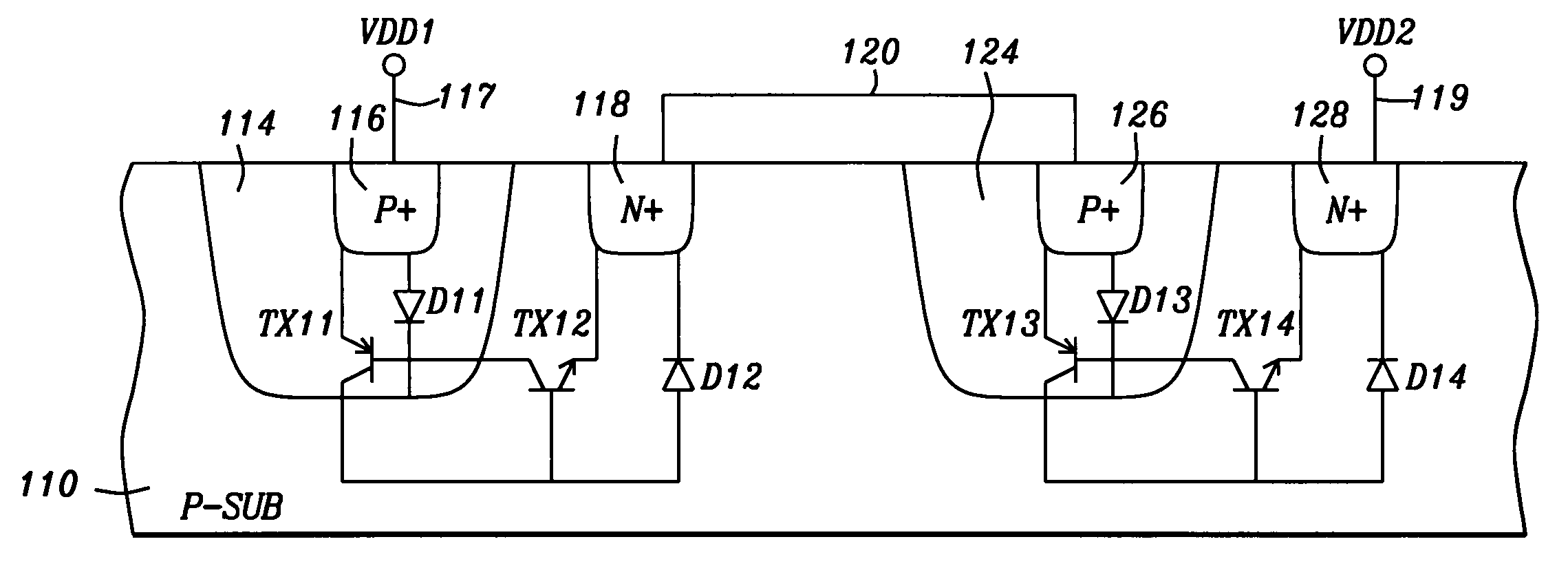
[0036]FIG. 3 shows the device structure arrangement of one embodiment of the invention. Starting with a P doped substrate 110, typically created on a single crystal silicon wafer of crystal orientation and with a typical doping level of between 1E15 and 5E15 a / cm3, processing is initiated as is well known in the art to define the active device areas.

[0037] After appropriate processing as is well understood in the art, an N-well is defined. This is typically done using a donor dopant such as phosphorous (P) in an ion implant process with an implant energy typically in the range of between 400 and 800 KeV and a dopant concentration of between 6E12 and 2E13 a / cm2. The resulting N-well has a typical dopant density of between 1E16 and 1E18 a / cm3.

[0038] Contained within the N-well 114 is a P+ contact 116. Again, this is created by methods well known in the art. One such method is ion implant with an acceptor element such as boron (B) in a dosage of between 1E15 and 5E15 a / cm2 and impla...


PUM


Abstract

The invention describes structures and a process for providing ESD protection between multiple power supply lines or buses on an integrated circuit chip. Special diode strings are used for the protection devices whereby the diodes are constructed across the boundary of an N-well and P substrate or P-well. The unique design provides very low leakage characteristics during normal circuit operation, as well as improved trigger voltage control achieved by stacking 2 or more diodes in a series string between the power buses.

Description

FIELD OF THE INVENTION [0001] The present invention relates generally to the structure and process for an ESD protection arrangement for ESD protection of single and multiple power supply feeds for integrated circuits and specifically to diode protection devices with associated parasitic bipolar transistors for power to power ESD protection. DESCRIPTION OF PRIOR ART [0002] Protection of integrated circuits from large, abnormal voltage or current surges such as caused by electrostatic discharge events (ESD) is increasingly important as device geometry is decreased. In particular the high impedance and relatively fragile gate oxide of field effect (FET) devices places further emphasis on the need for ESD protection. In addition multiple power lines often called power or voltage buses or rails require ESD protection with the protection devices affording minimum leakage between the various voltages levels and between the voltage levels and the reference level, typically ground. Some typ...

Claims


Application Information

Patent Timeline
IPC IPC(8): H01L21/331H01L23/62H01L27/02H01L29/78H01L33/00
CPCH01L27/0255
Inventor SHIH, JIAW-RENLEE, JIAN-HSING
Owner TAOWAM SEMICON MFG
Why Eureka
Try Eureka