
Semiconductor multilayer wiring board and method of forming the same

Inactive Publication Date: 2005-05-26
WASEDA UNIV +1
View PDF6 Cites 60 Cited by
  • Summary
  • Abstract
  • Description
  • Claims
  • Application Information

AI Technical Summary

Benefits of technology

[0021] As for forming an anti-diffusion film in the wiring-layer forming space formed through the dual damascene process in the silica-based interlayer insulating layer with its surface being processed, (i) the inner surface of the wiring-layer forming space may be processed with an organic-silane compound, thereby causing a film made of a monomolecular layer of the organic-silane compound to be adhesive; (ii) the surface of the monomolecular layer film has an excellent smoothness and can also be easily modified to be a catalyst with an aqueous solution containing a palladium compound; and (iii) the catalyst monomolecular layer film may be subjected to electroless plating, thereby forming a plated layer with a high copper-diffusion-preventive property on the monomolecular layer film. Thus, it has been confirmed that it is possible to form a thin anti-diffusion film with a high adhesiveness to the inner surface of the wiring-layer forming space and a high copper-diffusion-preventive property.

Problems solved by technology

Such a method of sequentially forming a multilayered wiring by repetition of lamination and etching requires a large number of steps, which tends to raise manufacturing cost.
That is, although copper is a suitable material as a conductive material for fine wiring because copper has an excellent electromigration resistance compared with aluminum, copper used to be unavailable in the conventional multilayer-wiring sequential forming method due to difficulty in etching.
With Cu in each wiring layer being diffused to the interlayer insulating layers 2, 8, and 10, the low dielectric property of the low-dielectric material forming the interlayer insulating layers is impaired, thereby causing an insulation defect.
Therefore, employment of spattering as described above which is a dry process upon making an anti-diffusion film and conductive layers is obviously not the best procedure.
However, if the wiring dimension is extremely finer, even with the use of a copper wiring having a small electrical resistance, an electric-signal speed is prone to decrease under the influence of the dielectric constant of the interlayer insulating film.
However, when not only the CVD method and the SOG method described above but also a technology disclosed in the patent document of “forming an anti-diffusion film by providing a palladium catalyst to an organic monomolecular film formed on an inner surface of a wiring-layer forming space formed by a dual damascene process” is applied to an interlayer insulating layer formed with a silica-based material (silica-based interlayer insulating layer), there may be several problems to be solved.
If such an Si—OH bond is not present on the surface of the interlayer insulating layer, forming a silane-based monomolecular layer film is difficult.” Another problem is how the surface of such an interlayer insulating layer should be processed.
Yet anther problem is in what way a monomolecular layer film of what type of structure should be formed on the surface of the processed silica-based interlayer insulating layer.
Yet another problem is which material is suitable as a material for giving a catalyzing activity to the monomolecular layer film.
Unless these problems are totally solved, it is impossible to provide a method of forming a semiconductor multilayer wiring board completely through a wet process from forming an interlayer insulating layer on a semiconductor substrate to embedding a wiring material in a wiring-layer forming space formed through a dual damascene process.
As of now, such a method has not been provided yet.

Method used


Image

  • Semiconductor multilayer wiring board and method of forming the same
  • Semiconductor multilayer wiring board and method of forming the same
  • Semiconductor multilayer wiring board and method of forming the same

Examples


example 1

Formation of the Semiconductor Multilayer Wiring Board and its Property

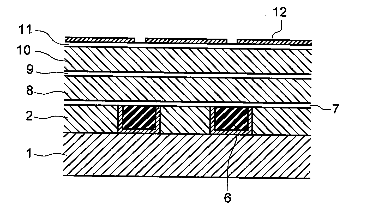
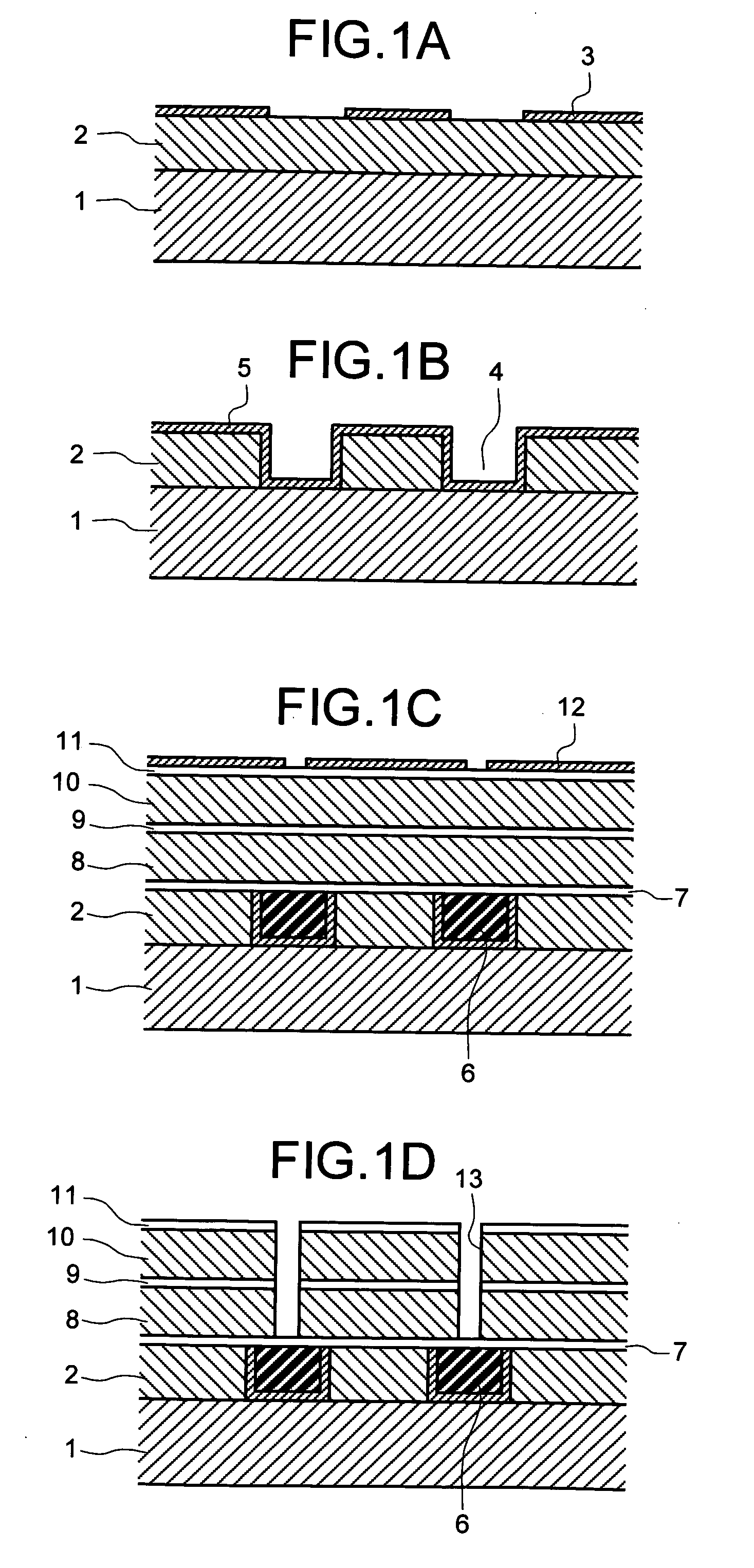
[0106] A spin-on-glass coating solution (manufactured by Tokyo Ohka Kogyo Co., Ltd. under the trade name of OCD T-12 800) whose principal component is a hydrolysate of trialkoxysilane as an inorganic SOG material was applied to a silicon substrate for 20 seconds by a spinner at 2000 rpm. Then, the substrate was dried on a hot plate at 80° C. for 1 minute, at 150° C. for 1 minute, and then at 200° C. for 1 minute. Then, the substrate was subjected to a heat processing under a nitrogen atmosphere at 450° C. for 30 minutes to obtain a coating film having a film thickness of 400 nanometers. The dielectric constant of the obtained silica-based interlayer insulating film was 3.0.

[0107] In the silica-based interlayer insulating film, a wiring-layer forming space was formed through a dual damascene process. Then, the substrate having formed thereon the silica-based interlayer insulating film was irradiated with an ultr...

examples 2 and 3

Evaluation of the Anti-Diffusion Property of the Anti-Diffusion Film in the Semiconductor Multilayer Wiring Board According to the Present Invention

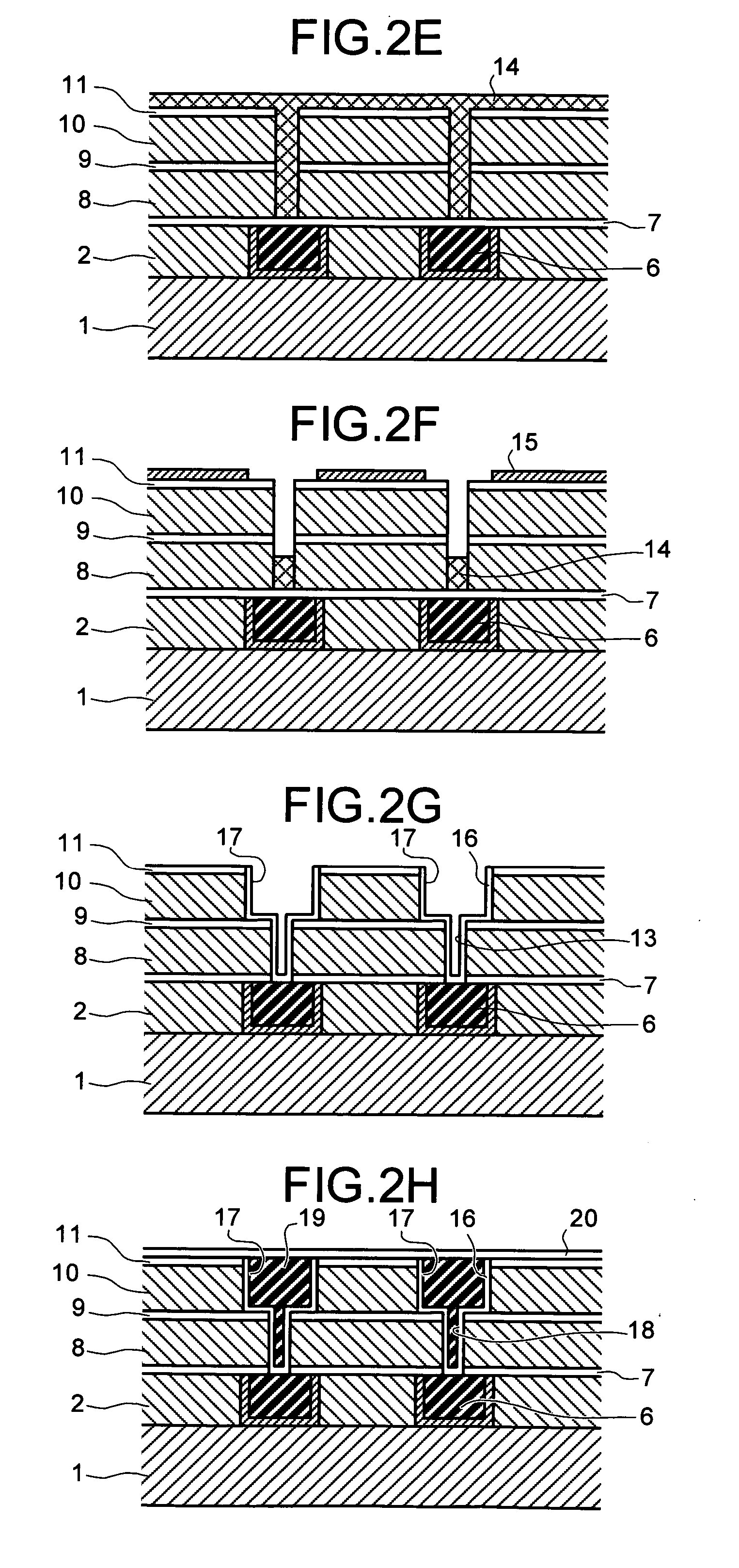
[0114] The spin-on-glass coating solution (manufactured by Tokyo Ohka Kogyo Co., Ltd. under the trade name of OCD T-12 800) was used as an inorganic SOG-based material to form a silica-based interlayer insulating layer. Then, by using a helium (He) plasma irradiating process and an ultraviolet irradiating process as a process for forming the Si—OH bond on the surface of the silica-based interlayer insulating layer, pseudo-models of the semiconductor multilayer wiring boards of the present invention were formed in the following manner. With the use of the formed pseudo-models, the anti-diffusion property of the anti-diffusion film in the semiconductor multilayer wiring board according to the present invention was evaluated. Although this pseudo-model did not include a wiring forming space, the anti-diffusion film in this pseudo-model was...

examples 4 and 5

Evaluation of the Anti-Diffusion Property of the Anti-Diffusion Film in the Semiconductor Multilayer Wiring Board According to the Present Invention

[0122] A spin-on-glass coating solution (manufactured by Tokyo Ohka Kogyo Co., Ltd. under the trade name of OCD T-9) whose principal component is a hydrolysate of methyltrialkoxysilane was used as an organic SOG-based material. Then, a process of forming the Si—OH bond on the surface of the silica-based interlayer insulating film was performed in the same manner as in Examples 2 and 3 except that an ultraviolet-ray irradiating process was the irradiation for 1 minute of an ultraviolet ray including a far-ultraviolet ray of 185 to 254 nanometers in the ambient atmosphere, thereby forming pseudo-models 3 and 4 of the semiconductor multilayer wiring boards of the present invention.

[0123] The obtained pseudo-models 3 and 4 of the semiconductor multilayer wiring boards of the present invention were subjected to annealing under a vacuum atmo...


PUM

PropertyMeasurementUnit
Electrical resistanceaaaaaaaaaa
Dielectric constantaaaaaaaaaa

Abstract

A silica-based interlayer insulating layer having a low dielectric constant is formed with SOG material on a substrate, in which a wiring-layer forming space is then formed. If necessary, a UV ray irradiation is performed under an oxidizing atmosphere. A Si—OH bond is formed on a surface of the insulating layer. A monomolecular layer film is then adhered to the inner surface of the space, which is then modified to be a catalyst with a solution containing Pd compound. On the catalyst monomolecular layer, a copper-diffusion-resistant film is formed by electroless plating, on which a copper plate is then formed as a wiring layer.

Description

BACKGROUND OF THE INVENTION [0001] 1) Field of the Invention [0002] The present invention relates to a semiconductor multilayer wiring board having a semiconductor multilayer wiring which has a lower wiring layer formed on a semiconductor substrate, and an upper wiring layer formed on the lower wiring layer via a interlayer insulating layer, in which the lower wiring layer and the upper wiring layer are connected to each other via a via-wiring vertically penetrating the interlayer insulating layer, as well as to a method of forming such a semiconductor multilayer wiring board. In more detail, the present invention relates to a semiconductor multilayer wiring board in which the via-wiring and the lower and upper wiring layers are formed by a simple dual damascene process and all layers from the interlayer insulating layer to the wiring layers are formed by a wet method, as well as to a method of forming such a semiconductor multilayer wiring board. [0003] 2) Description of the Relate...

Claims


Application Information

Patent Timeline
IPC IPC(8): C23C18/20C23C18/16C23C18/40C25D7/12H01L21/316H01L21/3205H01L21/4763H01L21/768H01L23/52H05K3/38H05K3/46
CPCH01L21/76801H01L21/76808H01L21/76814H01L21/76826H01L21/76831Y10T29/49155H01L21/76855H01L21/76864H01L21/76874H05K3/389H05K3/465H01L21/76843H01L21/3205
Inventor OSAKA, TETSUYAYOKOSHIMA, TOKIHIKOSATO, ISAOHASHIMOTO, AKIRAHAGIWARA, YOSHIO
Owner WASEDA UNIV
Features
  • Generate Ideas
  • Intellectual Property
  • Life Sciences
  • Materials
  • Tech Scout
  • Unparalleled Data Quality
  • Higher Quality Content
  • 60% Fewer Hallucinations
Learn More