Method of measuring pattern dimension and method of controlling semiconductor device process

a semiconductor device and pattern dimension technology, applied in the field of manufacturing techniques of semiconductor devices, can solve the problems of inability to precisely grasp which portion of the actual measurement dimension is actually measured, decreased measurement variance due to individual differences, and unnecessary expert skills of operators, so as to reduce the calculation amount, reduce the calculation time, and achieve the effect of precise pattern dimension measuremen

Active Publication Date: 2005-06-02
HITACHI HIGH-TECH CORP
View PDF1 Cites 24 Cited by
  • Summary
  • Abstract
  • Description
  • Claims
  • Application Information

AI Technical Summary

Benefits of technology

[0009] In the present invention, a highly precise pattern dimension measurement technique which is stable to the changes of the cross-sectional shapes of the pattern as mentioned above is provided, which has been difficult to be realized in the prior technique (technology concerning FIG. 15), and further, the pattern dimension measurement technique in which the calculation amount can be reduced in comparison to the above-mentioned technique (technology concerning FIG. 16) so as to reduce the calculation time. In addition, it is also possible to evaluate the changes in the cross-sectional shapes of the pattern in a quantitative manner. Further, it is also possible to realize a highly precise process control on the basis of these highly precise calculation results.
[0010] In a semiconductor pattern measurement method according to the present invention, the relationship between the cross-sectional shapes of the pattern and the measurement errors in a specified image processing technique are evaluated in advance, and in the actual dimension measurement, dimensions of an evaluation objective pattern are measured from the image signals of a scanning electron microscope, and errors of the dimensional measurement of the evaluation objective pattern are revised on the basis of the relationship between the cross-sectional shapes of the pattern and the measurement errors evaluated in advance. Further, in a pattern shape evaluation using tilt images, pattern shapes are evaluated in the same manner, and dimension measurement errors depending on the shapes are revised, thereby achieving the highly precise measurement.

Problems solved by technology

The measurement of pattern dimensions has been automated by applying image processing technologies to acquired images of the length measuring SEM, and therefore, expert skills of operators have become unnecessary, and measurement variance due to the individual differences has been decreased.
However, in these techniques, it is not possible to precisely grasp which portion an actually measured dimension corresponds to in an actual cross section (a top portion, a bottom portion or other of the pattern).
Especially, in the case where a cross-sectional shape of the pattern changes, errors in dimensions to be measured become different depending on the cross-sectional shape of the pattern, which has been a problem with the prior art.
Along with the scaling down in the semiconductor manufacturing processes, influences that the measurement errors according to the pattern shapes give to the process control have become more and more significant.
As a result, the amount of data will become enormous and it will take much time to prepare libraries.
Furthermore, in the measurement, the prepared waveforms must be compared with actual waveforms, and therefore, calculations take much more time than conventional measurement techniques.

Method used


Image

  • Method of measuring pattern dimension and method of controlling semiconductor device process
  • Method of measuring pattern dimension and method of controlling semiconductor device process
  • Method of measuring pattern dimension and method of controlling semiconductor device process

Examples


first embodiment

(Entire Process Flow)

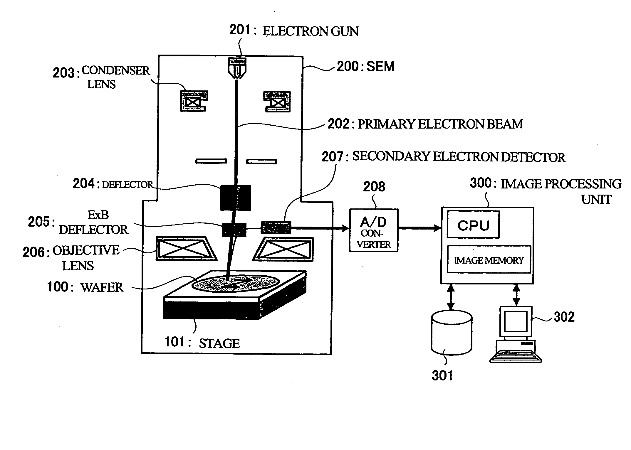
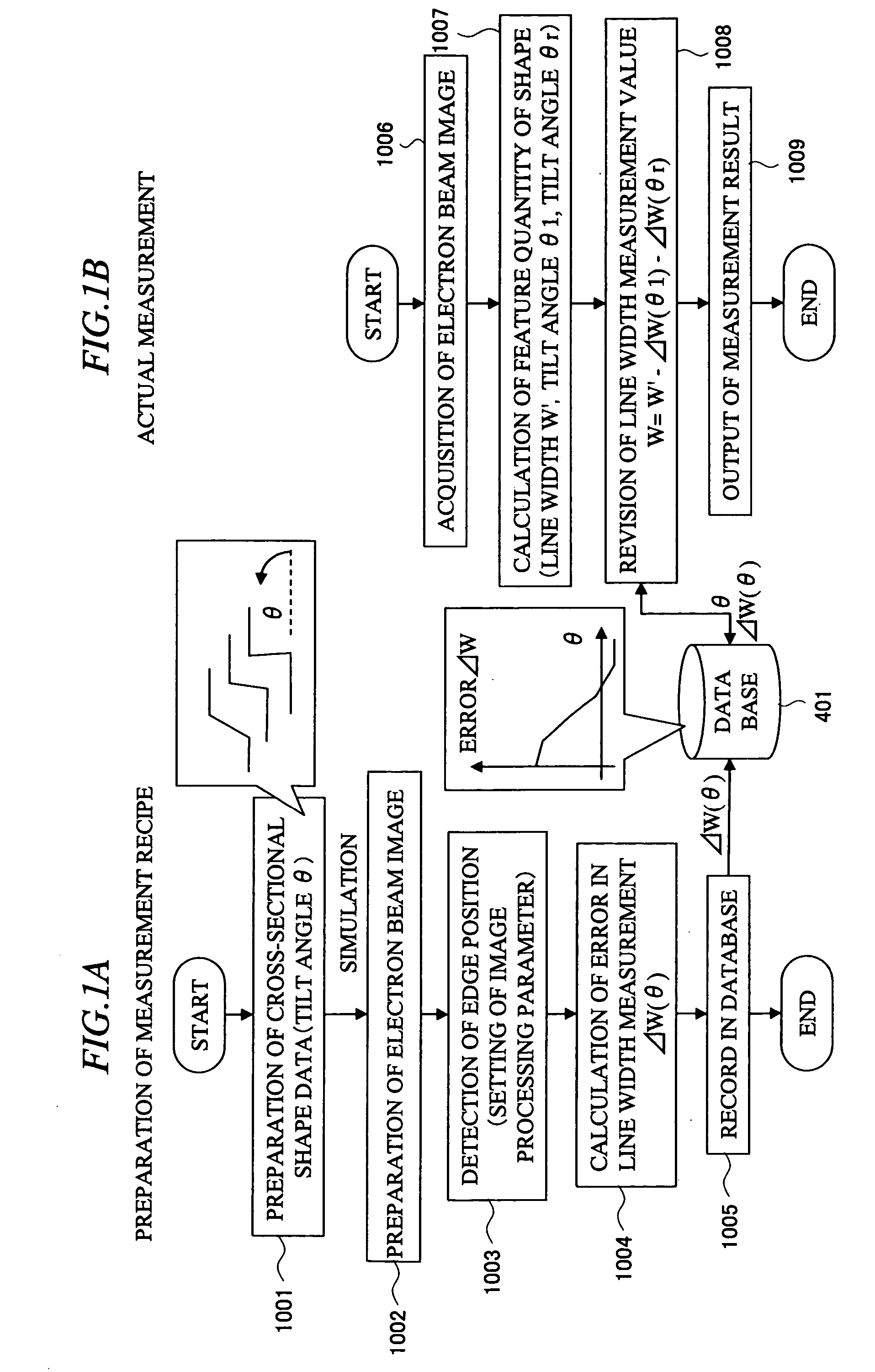
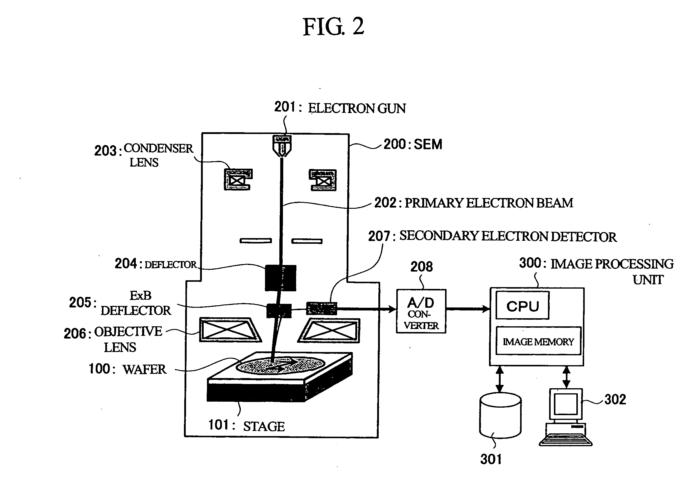
[0034]FIG. 1 is a schematic diagram of measurement procedures using a pattern measurement system established on a length measuring SEM 200 (whose schematic structure is shown in FIG. 2) in a first embodiment of the present invention. In an example of this embodiment, two steps are required, that is, the measurement recipe preparing step for preparing a measurement recipe in which measurement conditions and procedures for the automatic measurement are recorded (FIG. 1A), and the step of actually measuring a measurement objective pattern (FIG. 1B).

[0035] First, the procedures in the step of preparing measurement recipe (FIG. 1A) will be described below. When preparing the measurement recipe, a database 401 in which the relationship between the cross-sectional shapes of a measurement objective pattern and dimension measurement errors is recorded is prepared. In the example of FIG. 1, a method using an electron beam simulation will be described.

[0036] First, cro...

second embodiment

hment by Actual Sample or AFM

[0058] Next, a second embodiment will be described with reference to FIG. 8. In the first embodiment, a database of the relationship between the cross-sectional shapes of the pattern and the dimension measurement errors is established by the use of an electron beam simulation. However, in the second embodiment, an example is shown, in which patterns of various shapes are prepared actually and a database is established by the use of images of these patterns observed actually by SEM.

[0059]FIG. 8 shows the procedures of establishing the database. First, patterns for simulating the actually possible process variations according to plural process conditions (exposure condition for a resist pattern, etching condition for an etching pattern, and so forth) are formed (step 1020). Further, SEM images of these patterns are acquired under the same conditions as those at the actual measurement (step 1021), and position detection (dimension measurement) of each edge...

third embodiment

etry

[0061] Next, a third embodiment will be described with reference to FIG. 9. In the first embodiment, a database of the relationship between the cross-sectional shapes of the pattern and the dimension measurement errors is established by the use of an electron beam simulation, and the evaluation of the solid shapes of objective patterns is carried out by the use of the feature quantity of the image obtained from SEM images. However, in the third embodiment, an example is shown, in which the establishment of a database and the evaluation of the cross-sectional shape of the pattern in the measurement are carried out by the use of scatterometry (shape evaluation technique using scattered light).

[0062] The establishment of a database is carried out in the same manner as in the second embodiment, while the evaluation of cross-sectional shape (step 1030) is carried out not by the cross section observation or AFM but by the scatterometry. In the measurement, first, the evaluation of cr...


PUM

PropertyMeasurementUnit
tilt angleaaaaaaaaaa
diffusion lengthaaaaaaaaaa

Abstract

This invention provides a method of measuring semiconductor pattern dimensions capable of realizing a stable and highly precise pattern dimension measurement technique even when the pattern cross-sectional shapes are changed and making the calculation amount relatively small to reduce the calculation time. More specifically, the relationship between cross-sectional shapes of a pattern and measurement errors in a specified image processing technique is evaluated in advance by the electron beam simulation in a pattern measurement system in a length measuring SEM, and in the actual dimension measurement, dimensions of an evaluation objective pattern are measured from image signals of a scanning electron microscope, and errors of the dimensional measurement of the evaluation objective pattern are estimated and revised based on the relationship between cross-sectional shapes of a pattern and measurement errors evaluated in advance, thereby realizing highly precise measurement where dimensional errors depending on pattern solid shapes are eliminated.

Description

CROSS-REFERENCE TO RELATED APPLICATION [0001] The present application claims priority from Japanese Patent Application JP 2003-397364 filed on Nov. 27, 2003, the content of which is hereby incorporated by reference into this application. TECHNICAL FIELD OF THE INVENTION [0002] The present invention relates to a manufacturing technique of a semiconductor device. More specifically, it relates to a technique effectively applied to a method and a system for evaluating processed shape conditions of a circuit pattern formed on a wafer by the use of electron beam images of the circuit pattern in a semiconductor manufacturing process. BACKGROUND OF THE INVENTION [0003] Examinations by the inventors of the present invention have learned that measurement and control of pattern dimensions by the use of an electronic microscope exclusive for the measurement (length measuring SEM) is generally conducted today in the semiconductor manufacturing processes. The measurement of pattern dimensions has...

Claims


Application Information

Patent Timeline
Patent Type & Authority Applications(United States)
IPC IPC(8): G01B11/14G01B15/00G01N23/225H01J37/28H01J37/304H01L21/66
CPCH01J37/28H01J37/304H01J2237/30455H01J2237/2817H01J2237/2814
Inventor TANAKA, MAKIMOROKUMA, HIDETOSHISHISHIDO, CHIETAKAGI, YUJI
Owner HITACHI HIGH-TECH CORP
Why Eureka
Try Eureka