Circular polarization spin semiconductor laser using magnetic semiconductor and laser beam generating method

a laser and semiconductor technology, applied in the direction of lasers, laser output parameters control, semiconductor lasers, etc., can solve the problems of high-power circularly polarized laser light based on current injection that has not been obtained, and achieve enhanced emission efficiency, high efficiency, and high efficiency

Inactive Publication Date: 2005-06-02
JAPAN SCI & TECH CORP
View PDF3 Cites 15 Cited by
  • Summary
  • Abstract
  • Description
  • Claims
  • Application Information

AI Technical Summary

Benefits of technology

[0053] Based on a magnetic semiconductor prepared by doping either one of ZnO, group II-VI compound semiconductor and group III-V compound semiconductor, with transition metal atoms having a controlled concentration, a pair of p-type and n-type half-metal ferromagnetic semiconductor layers are formed by doping the magnetic semiconductor, respectively, with an acceptor and a donor. Alternatively, the p-type and n-type half-metal ferromagnetic semiconductor layers are designed to have an insulated-gate field effect transistor-like structure and utilize the field effect induced by gate voltages different in magnitude and positive / negative sign. Then, through current injection, a flow of spin-coherent holes polarized in one of spin directions, and a flow of spin-coherent electrons polarized in the other spin direction opposite to that of the holes, are created, respectively, in the p-type and n-type half-metal ferromagnetic semiconductor layers, to combine the electrons and holes which have entered, respectively, into the conduction band and the valence band in opposite spin directions, with high efficiency, through the active layer with a multi-quantum well structure capable of adjusting the bandgap, so that a completely (100%) circularly polarized CW (Continuous Wave) laser light can be generated according to the selection rule.
[0054] This function will be described in detail with reference to an energy diagram illustrated in FIG. 1. In FIG. 1, an active layer with a multi-quantum well structure defined by a CBM (Conduction Band Minimum: the bottom of the conduction band) and a VBM (Valence band Maximum: the top of the valence band) and a cladding layer to be disposed on the side of each of p-type and n-type regions are sandwiched between p-type and n-type completely spin-polarized magnetic semiconductor layers. This laser source is designed to generate a light from both the multi-quantum well structure and the cladding layers so as to provide enhanced emission efficiency. A hole h and electron e polarized in opposite spin directions and injected from the p-type and n-type magnetic semiconductor layers as indicated by the arrows can be combined together with high efficiency while maintain them in the opposite spin directions, to generate a completely circularly polarized laser light hv. The enhanced combination between the electron and the hole in an actual space, and the exciton binding energy of ZnO (60 meV), GaN (24 meV) or the like, allow the emission to be performed with high efficiency.

Problems solved by technology

Despite expectations to various industrial uses of a circularly polarized light-generating spin-based semiconductor laser source (hereinafter referred to as “circular-polarization spin-based semiconductor laser source”), such as applications to production technologies, information / communications technologies, spectroscopies, nanotechnologies or quantum manipulations, any high-power circularly polarized laser light based on current injection has not been obtained, because it has been unable to prepare a completely (or 100%) spin-polarized p-type or n-type semiconductor.

Method used


Image

  • Circular polarization spin semiconductor laser using magnetic semiconductor and laser beam generating method
  • Circular polarization spin semiconductor laser using magnetic semiconductor and laser beam generating method
  • Circular polarization spin semiconductor laser using magnetic semiconductor and laser beam generating method

Examples


embodiment

First Embodiment

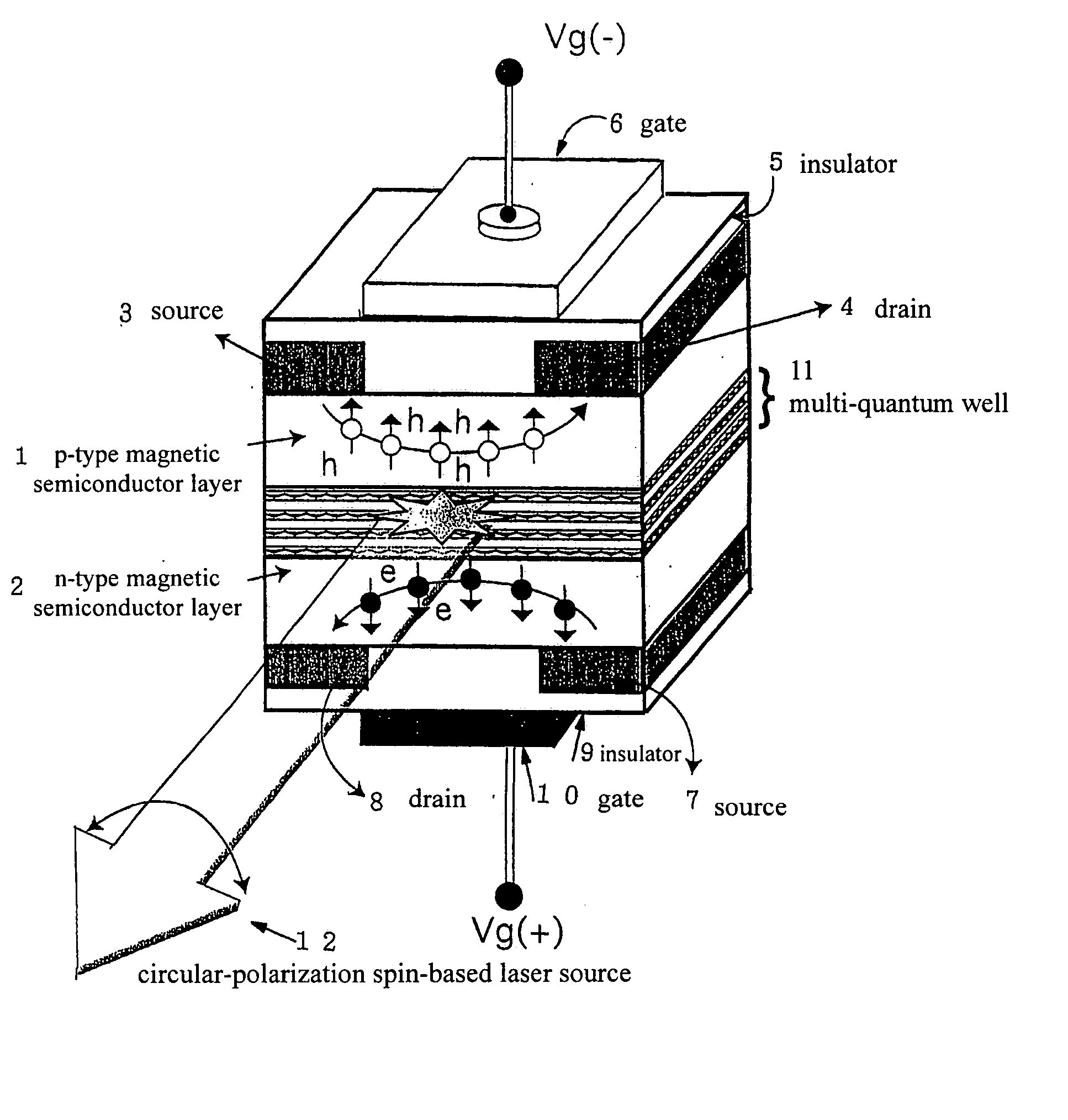
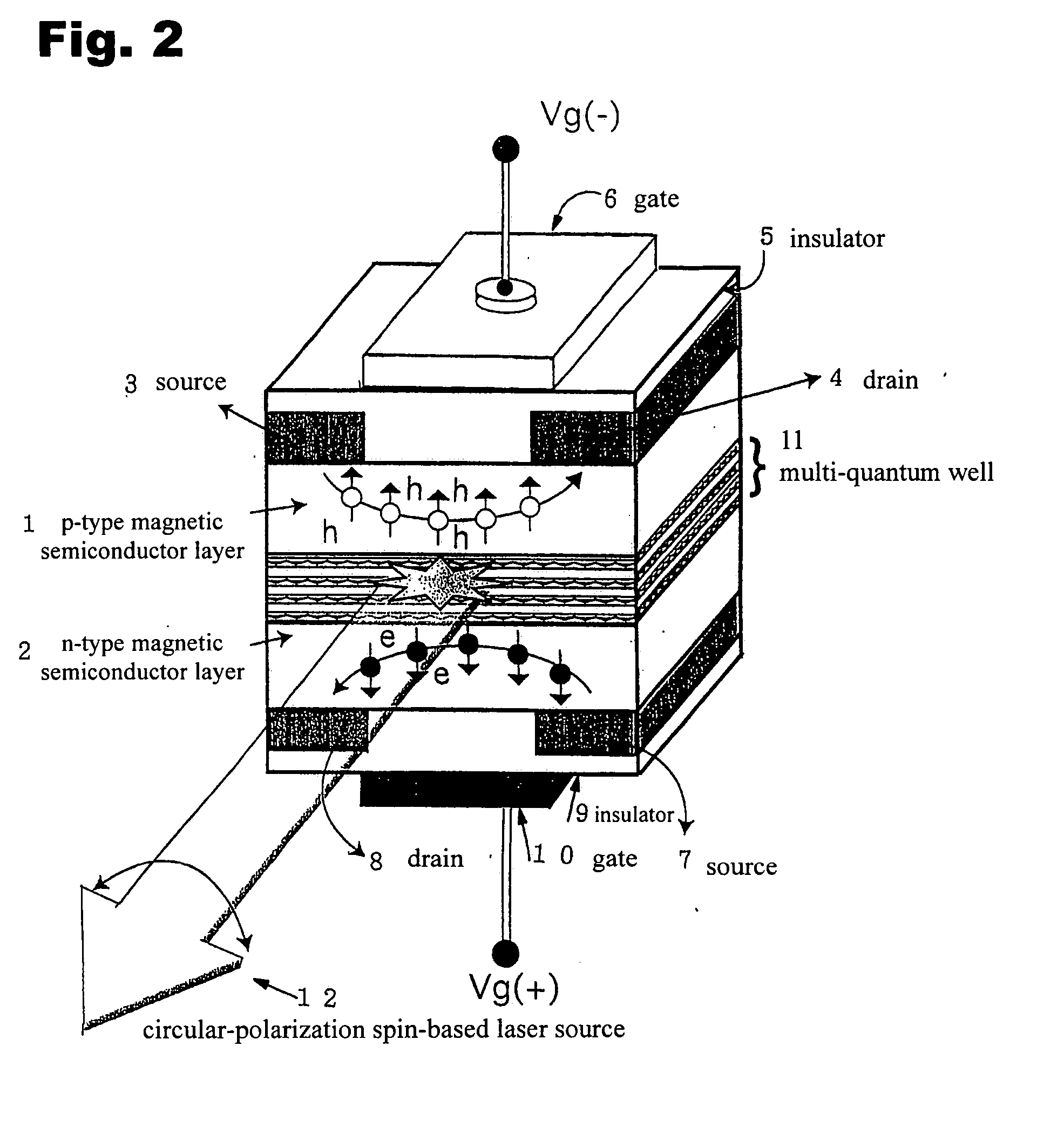
[0084]FIG. 2 is a schematic diagram showing the structure of the current-injection type circular-polarization spin-based semiconductor laser source 1 utilizing the field effect induced by a gate bias, according to the first embodiment of the present invention.

[0085] As shown in FIG. 2, a source 3, a drain 4 and a gate insulator 5 are provided on the upper surface of a p-type half-metal ferromagnetic semiconductor layer 1, and a gate 6 is provided on the gate insulator 5 in a contact manner. In this manner, the p-type half-metal ferromagnetic semiconductor layer (p-type DMS layer) 1 is operable, in response to the gate voltage, to receive holes and inject the holes all of which have spins uniformed in one direction based on its ferromagnetic half-metal state, from the source having a spin domain direction pinned by a magnetic field or an antiferromagnetic superlattice thin film.

[0086] A source 7, a drain 8 and a gate insulator 9 are provided on the lower surface of...

second embodiment

[0089]FIG. 5 is a schematic diagram showing the structure of the current-injection type circular-polarization spin-based semiconductor laser source 1 according to the first embodiment of the present invention.

[0090] As shown in FIG. 5, an active layer with a multi-quantum well structure 11 is sandwiched by a p-type magnetic semiconductor layer 1 and an n-type magnetic semiconductor layer 2. Further, in order to provide enhanced emission efficiency, a laminated structure is formed by sandwiching the multi-quantum structure 11 between a p-type cladding layer 13 and an n-type cladding layer 14. This laminated structure is provided on a substrate 15 through a buffer layer 16. Further, an electrode 17 is provided on the p-type magnetic semiconductor layer 1, and an electrode 18 is provided on the n-type magnetic semiconductor layer 2.

[0091] Specifically, through a MBE Process, a low-temperature grown buffer layer made of n-type GaN doped with Si at 400° C. was grown on an Al2O3 substra...


PUM


Abstract

Disclosed is a spin-based semiconductor laser source capable of generating a completely circularly polarized laser light by injecting current into p-type and n-type half-metal magnetic semiconductor layers. Each of the p-type and n-type half-metal magnetic semiconductor layers is prepared by doping a magnetic semiconductor with a transition metal atom and optionally with an acceptor or donor. Alternatively, each of the p-type and n-type half-metal magnetic semiconductor layers is prepared by providing a gate to a magnetic semiconductor and adjusting / controlling its ferromagnetic state according to the field effect. The present invention can solve the problem concerning the insufficient degree of circular polarization in conventional circular-polarization semiconductor laser sources.

Description

TECHNICAL FIELD [0001] The present invention relates to a circularly polarized light-generating spin-based semiconductor laser source using a magnetic semiconductor, and a method of generating a laser light using the laser source. BACKGROUND ART [0002] A semiconductor laser source has excellent compactness and conformance to highly integrated semiconductor devices. In late years, a wide-bandgap semiconductor material opens the way for developments of higher-power semiconductor laser sources with an oscillation wavelength of up to the ultraviolet range. [0003] A magnetic-semiconductor laser source has been known for quite some time (for example, the following Patent Publication 1). There has also been known a semiconductor laser source capable of generating a circularly polarized laser light having a specific polarization direction. [0004] For example, the following Patent Publication 2 discloses an optical semiconductor device in which an electrode made of magnetic material or magne...

Claims


Application Information

Patent Timeline
Patent Type & Authority Applications(United States)
IPC IPC(8): H01S5/32H01S5/06H01S5/30H01S5/343H01S5/347
CPCB82Y20/00H01S5/0607H01S5/305H01S2301/14H01S5/3086H01S5/343H01S5/347H01S5/3068H01S5/32
Inventor YOSHIDA, HIROSHISATO, KAZUNORI
Owner JAPAN SCI & TECH CORP
Why Eureka
Try Eureka