Layered structures

a layer structure and structure technology, applied in the field of layer structures, can solve the problems of complex process, limited types and concentrations of ions which can be successfully implanted in diamonds, and permanent degradation of important properties, so as to reduce the amount of post-growth processing complexity.

Inactive Publication Date: 2005-06-02
WHITEHEAD ANDREW JOHN +2
View PDF4 Cites 38 Cited by
  • Summary
  • Abstract
  • Description
  • Claims
  • Application Information

AI Technical Summary

Benefits of technology

[0024] The process of the invention minimises excessive complicated post growth processing and enables structures that contain thin layers of diamond with properties very different to a second thicker layer to be synthesised. These structures have, for example, use in electronic applications.

Problems solved by technology

This method has the disadvantage that damage to the diamond occurs during ion implantation which can result in permanent degradation in important properties such as carrier lifetimes and mobilities.
Further, the types and concentration of ions which can be successfully implanted in diamond are limited and the process often requires complex post implantation annealing.
A CVD process is conducive to the synthesis of thin epi layers but has the disadvantage that only layers containing certain dopants can be synthesised.
For example it is well known that HPHT synthesis provides a method of incorporating nickel, cobalt and nitrogen into the diamond in high concentrations (>5 parts per million (ppm) carbon atoms) but to date this has not been possible using CVD methods.
Furthermore, ion implantation doping is always associated with lattice damage due to the ion implantation, which substantially reduces the benefit obtained from the dopant in that it adversely modifies the electronic properties of the doped layer.

Method used


Image

  • Layered structures
  • Layered structures

Examples


example 1

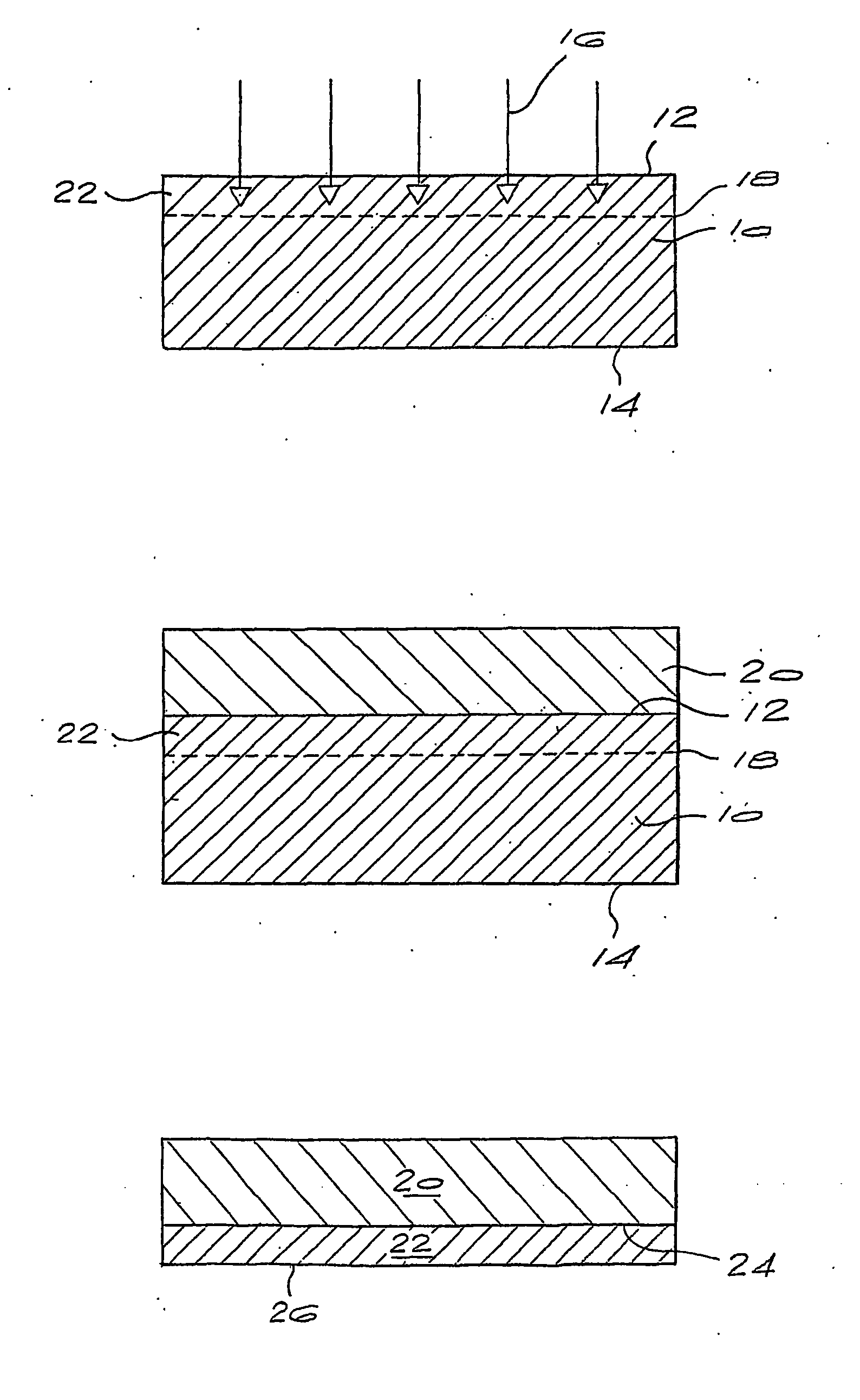
[0032] A high purity diamond substrate produced using a CVD method known in the art with thickness 600 μm, is first implanted with 2 MeV oxygen ions to a dose of 1×1017 cm−2. A thick (300 μm) boron doped single crystal CVD layer which has, as measured by SIMS, 2×10¹⁹ B atoms / cm−3 is grown on a surface of this substrate. Following growth the layered product is electrochemically etched to produce two samples: (i) a high purity diamond layer that can be reused and (ii) a two layer product consisting of a 1 μm high purity diamond layer and a 300 μm boron doped diamond layer in contact with the high purity diamond layer. This two layer product has an electronic application.

example 2

[0033] A boron doped (1×1019 cm−3) diamond substrate prepared using a CVD method with thickness 620 μm is first implanted with 2 MeV hydrogen ions to a dose of 1×1019 cm−2. A thick (300 μm) high purity single crystal CVD diamond layer is grown on to a surface of this substrate. Following growth the layered product is electrochemically etched to produce two samples: (i) a boron doped diamond plate which can be reused, and (ii) a two layer product consisting of a 10 μm boron doped diamond layer and a 300 μm high purity diamond layer. This two layer product has an electronic application.


PUM

PropertyMeasurementUnit
energyaaaaaaaaaa
depthaaaaaaaaaa
depthaaaaaaaaaa

Abstract

A process of making a product which comprises at least two layers in contact with each other, each layer being of a wide-gap material and each layer differing from each other in at least one property, includes the steps of: (i) providing a substrate of a wide-band gap material having a surface and a region adjacent the surface having a particular characteristic, (ii) ion implanting the substrate through the surface to form a damaged layer below that surface, (iii) growing a layer of a wide-band gap material by chemical vapour deposition on at least a portion of the surface of the substrate through which ion implantation occurred, the material of the grown layer having a characteristic different to that of the region of the substrate adjacent the surface through which ion implantation occurred, and (iv) severing the substrate through the damaged layer. The wide-gap material is preferably diamond.

Description

BACKGROUND OF THE INVENTION [0001] This invention relates to layered structures, particularly layered diamond structures. [0002] For certain diamond applications, it is necessary to have two or more layers of diamond which have different properties in atomic contact with each other. One example is in electronics where a layered structures can be used to make a device, for example as described in WO 01 / 18882 A1 [0003] One method of making a layered diamond structure is by using ion implantation. Ions may be implanted into diamond to create an n-type or p-type semi-conducting layer on top of a layer with a different property. This method has the disadvantage that damage to the diamond occurs during ion implantation which can result in permanent degradation in important properties such as carrier lifetimes and mobilities. Further, the types and concentration of ions which can be successfully implanted in diamond are limited and the process often requires complex post implantation annea...

Claims


Application Information

Patent Timeline
Patent Type & Authority Applications(United States)
IPC IPC(8): C23C14/58C23C16/01C23C14/48C30B33/00H01L21/04H01L21/20H01L21/265
CPCC23C16/01C30B33/00H01L21/0405H01L21/041H01L29/66022C30B29/60
Inventor WHITEHEAD, ANDREW JOHNTWITCHEN, DANIEL JAMESSCARSBROOK, GEOFFREY ALAN
Owner WHITEHEAD ANDREW JOHN
Why Eureka
Try Eureka