Organic electroluminescent devices

a light-emitting diode and electroluminescent technology, applied in the direction of discharge tube luminescnet screens, sustainable buildings, natural mineral layered products, etc., can solve the problems of large loss of efficiency, difficult control, and performance limitations that have been a barrier to many desirable applications, and achieve the effect of useful white light emission

Inactive Publication Date: 2005-06-09
EASTMAN KODAK CO
View PDF11 Cites 458 Cited by
  • Summary
  • Abstract
  • Description
  • Claims
  • Application Information

AI Technical Summary

Benefits of technology

[0016] Such devices provide useful white light emissions.

Problems solved by technology

While organic electroluminescent (EL) devices have been known for over two decades, their performance limitations have represented a barrier to many desirable applications.
However, it is generally believed that only 25% of the excitons created in an EL device are singlet excitons.
This results in a large loss in efficiency since 75% of the excitons are not used in the light emission process.
These concentrations are difficult to control during large-scale manufacturing.
However, the color filters each transmit only about 30% of the original white light.
Also there is a problem in the application of white OLEDs, when used with color filters, in that the intensity of the red, green or blue component of the emission spectrum is frequently lower than desired due to the low transmission of the band pass filter.

Method used


Image

  • Organic electroluminescent devices
  • Organic electroluminescent devices
  • Organic electroluminescent devices

Examples


synthetic example 1

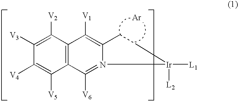
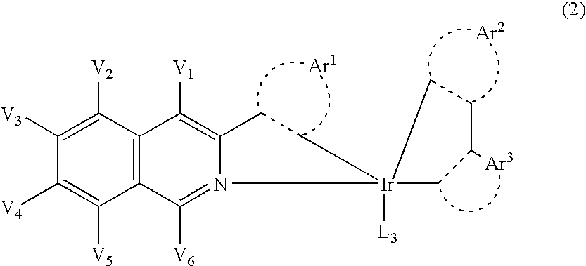
The Synthesis of 3-Phenylisoquinoline and Iridium Complexes of 3-Phenylisoquinoline

[0158]

[0159] 3-Phenylisoquinoline was prepared by the following procedure (see Huang et al., J. Org. Chem. 67, 3437 (2000), Rxn-1). A round bottom flask containing N-(2-phenylethynylbenzylidene)-t-butyl-amine (12.7 g, 48.6 mmol) was dissolved in anhydrous DMF under a nitrogen blanket. Cuprous iodide was added and the reaction vessel was warmed to 100° C. After three hours, thin layer chromatography (dichloromethane eluant) indicated no remaining starting material. One major product was formed. The reaction mixture was cooled to room temperature and the DMF removed by distillation. The residue was taken up in dichloromethane and washed with water, brine and the organic solution dried over magnesium sulfate. Solvents were evaporated to yield 9.9 grams of crude product. This material was further purified by flash chromatography on 800 grams of silica-gel with dichloromethane as eluant. The collected fra...

example 1

Device Example 1

Evaluation of Phosphorescent Light Emitting Materials

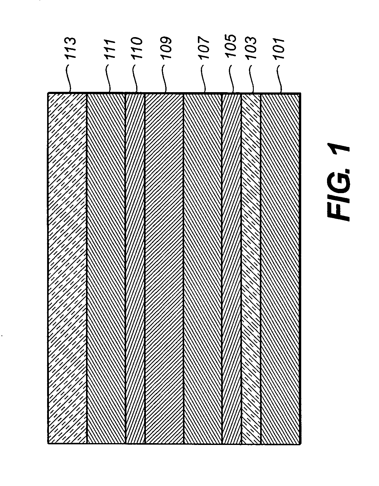
[0163] Phosphorescent light-emitting materials were evaluated to determine if they would provide good operating lifetimes and hues. An EL device (Sample 1) was constructed in the following manner:

[0164] 1. A glass substrate coated with an 85 nm layer of indium-tin oxide (ITO) as the anode was sequentially ultrasonicated in a commercial detergent, rinsed in deionized water, degreased in toluene vapor and exposed to oxygen plasma for about 1 min.

[0165] 2. Over the ITO was deposited a 1 nm fluorocarbon (CFx) hole-injecting layer (HIL) by plasma-assisted deposition of CHF3.

[0166] A hole-transporting layer (HTL) of N,N′-di-1-naphthyl-N,N′-diphenyl-4,4′-diaminobiphenyl (NPB) having a thickness of 75 nm was then evaporated from a tantalum boat.

[0167] 3. A 35 nm light-emitting layer (LEL) of 4,4′-N,N′-dicarbazole-biphenyl (7a, CBP) and 8 wt. % fac-tris(3-phenyl-isoquinolinato) iridium (III) were then deposited onto th...

example 2

Device Example 2

[0182] An EL device (Sample 11) satisfying the requirements of the invention was constructed in the following manner:

[0183] 1. A glass substrate coated with an 85 nm layer of indium-tin oxide (ITO) as the anode was sequentially ultrasonicated in a commercial detergent, rinsed in deionized water, degreased in toluene vapor and exposed to oxygen plasma for about 1 min.

[0184] 2. Over the ITO was deposited a 1 nm fluorocarbon (CFx) hole-injecting layer (HIL) by plasma-assisted deposition of CHF3.

[0185] 3. A hole-transporting layer (HTL)of N,N′-di-1-naphthyl-N,N′-diphenyl-4,4′-diaminobiphenyl (NPB) having a thickness of 95 nm was then evaporated from a tantalum boat.

[0186] 4. A 20 nm first light-emitting layer (LEL) of host 8c and 2.5 wt. % blue light-emitting material (5c) were then deposited onto the hole-transporting layer. These materials were also evaporated from tantalum boats.

[0187] 5. A 20 nm second LEL of 4,4′-N,N′-dicarbazole-biphenyl (7a, CBP) and 8 wt. % ...


PUM

PropertyMeasurementUnit
thickaaaaaaaaaa
quantum efficienciesaaaaaaaaaa

Abstract

Disclosed is an electroluminescent device comprising a cathode and anode, and therebetween, at least two light-emitting layers wherein the first layer, layer A, comprises a phosphorescent light-emitting organometallic compound comprising iridium and an isoquinoline group and a second layer, layer B, comprising a light-emitting material. Such devices provide useful white light emissions.

Description

FIELD OF THE INVENTION [0001] This invention relates to an organic light-emitting diode (OLED) electroluminescent (EL) device comprising a cathode and anode, and therebetween, at least two light-emitting layers wherein the first layer, layer A, comprises a phosphorescent light-emitting organometallic compound comprising iridium and an isoquinoline group and a second layer, layer B, comprising a light-emitting material. BACKGROUND OF THE INVENTION [0002] While organic electroluminescent (EL) devices have been known for over two decades, their performance limitations have represented a barrier to many desirable applications. In simplest form, an organic EL device is comprised of an anode for hole injection, a cathode for electron injection, and an organic medium sandwiched between these electrodes to support charge recombination that yields emission of light. These devices are also commonly referred to as organic light-emitting diodes, or OLEDs. Representative of earlier organic EL de...

Claims


Application Information

Patent Timeline
Patent Type & Authority Applications(United States)
IPC IPC(8): C09K11/06H01L51/00H01L51/30H01L51/50H05B33/14
CPCC09K11/06Y02B20/181C09K2211/1011C09K2211/1014C09K2211/1029C09K2211/1033C09K2211/1037C09K2211/107C09K2211/1092C09K2211/185H01L51/0059H01L51/0062H01L51/0081H01L51/0085H01L51/5016H01L51/5036H05B33/14C09K2211/1007Y02B20/00H10K85/649H10K85/631H10K85/324H10K85/342H10K50/125H10K50/11H10K2101/10
Inventor DEATON, JOSEPH C.HATWAR, TUKARAM K.KONDAKOV, DENIS Y.BROWN, CHRISTOPHER T.
Owner EASTMAN KODAK CO
Why Eureka
Try Eureka