

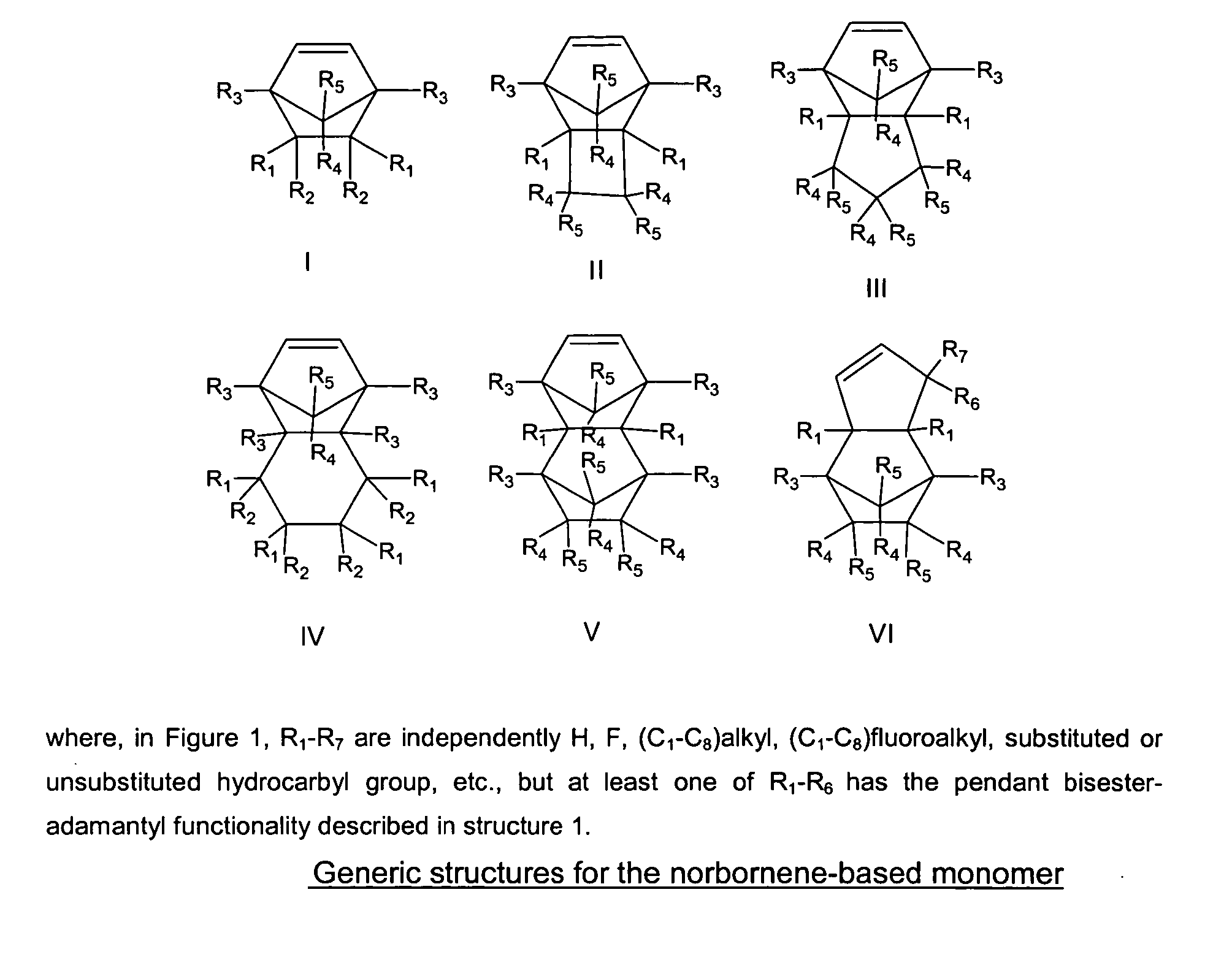
Photoresist composition for deep UV and process thereof
a technology of composition and resist, applied in the field of photoresist composition, can solve the problems of high etch rate, inability to use open-chain aliphatic resins, and inapplicable photoresist materials for 248 nm,
- Summary
- Abstract
- Description
- Claims
- Application Information
AI Technical Summary
Problems solved by technology
Method used
Image

Examples
example 1
Synthesis of 2-methyl-2-adamantyl Acetyl Norbornene Carboxylate (MAdoc ME)
[0060] Norbornene carboxylic acid (9.8 g) was taken into a 250 ml round bottom reaction flask, along with the bromo acetyl-2-methyl-2-adamantyl (10.0 g) and 100 ml of dry tetrahydrofuran (THF). The flask was stirred using an overhead stir motor driving a glass shaft with Teflon blade. It was mixed slowly until everything was dissolved in THF, yielding a clear uniform liquid. Then triethylamine (3.58 g,) was added drop wise. A large amount of white precipitate was formed. The mixture was allowed to mix overnight; the white solid was filtered and then washed with THF. The solid collected was discarded. The THF solution was drowned in ether (200-300 ml). The mixture was then washed with 5% HCl, 2×100 ml, and then washed with 5% K2CO3, 2×100 and water 2×100 ml. The organic phase was dried over Na2SO4. sodium sulphate was filterd and discarded and the filtrate was evaporated under vacuum. The reaction yielded 9.1 ...
example 2
Poly(Norbornene MAdoc ME-co-β-methacryloyloxy-γ-butyolactone-co-2-methyladamantyl methacrylate-co-methacryloyloxy-norbornane-butyrolactone-co-maleic Anhydride)
[0061] A hybrid copolymer was synthesized by reacting 8.16 g of norbornene MAdoc ME (10 mole %) from Example 1, 24.15 g of β-methacryloyloxy-γ-butyolactone (GBLMA, 30 mole %), 22.19 g of 2-methyladamantyl methacrylate (MAdMA, 40 mole %), 5.26 g of methacryloyloxy-norbornane-butyrolactone (MNBL, 10 mole %) and 2.32 g of maleic anhydride (MA) in the presence of 5 weight % of 2,2′azobisisobutyronitrile (AIBN) in tetrahydrofuran (THF) at 50% solid. The reaction was carried out for 7 hours and the polymer was isolated from diethyl ether twice (1 / 10 v / v ratio), giving a yield of 33.4 g (66.7%). The weight average molecular weight (Mw) as measured on a Gel Permeation Chromatograph (GPC) using polystyrene standards and THF solvent was 16,110.
example 3
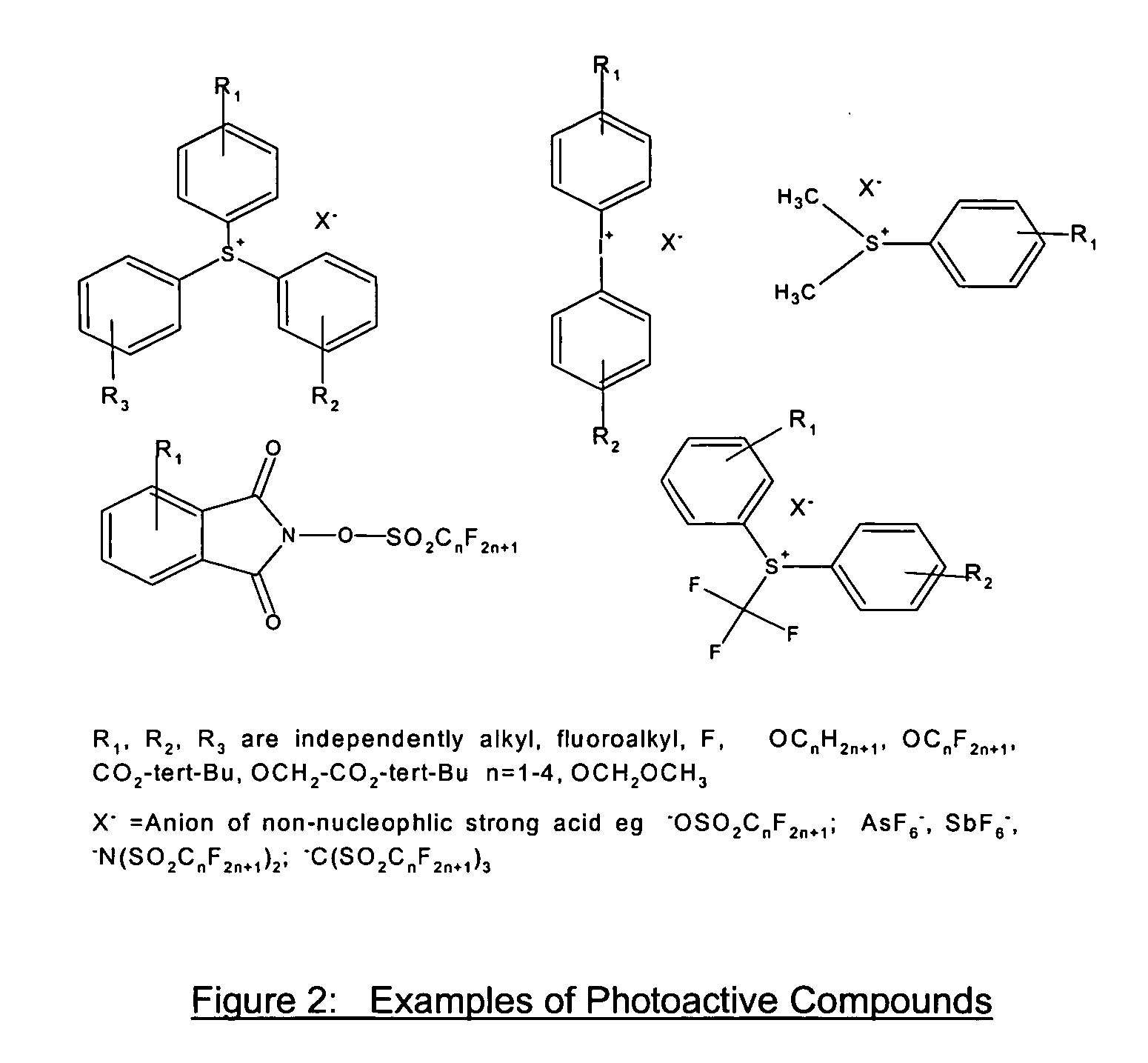
[0062] 2.4646 g of polymer from example 2; 0.0416 g (30 μmol / g) of triphenylsulfonium nonafluorobutane sulfonate, 0.0416 g (30 μmol / g) of 4-methoxy-3,5-dimethyl phenyl dimethyl sulphonium nonaflate, 0.7149 g of 1 weight % PGMEA solution of N-(1-adamantyl acetamide) and 0.0371 g of 10 weight % PGMEA solution of a surfactant (fluoroaliphatic polymeric ester, supplied by 3M Corporation, St. Paul Minn.) were dissolved in 26.1588 g of PGMEA, and 0.5502 g of gamma valerolactone to give a 30 g photoresist solution.
[0063] Separately, a silicon substrate coated with a bottom antireflective coating (B.A.R.C.) was prepared by spin coating the bottom anti-reflective coating solution (AZ® EXP ArF-1 B.A.R.C. available from Clariant Corporation, Somerville, N.J.) onto the silicon substrate and baking at 175° C. for 60 sec. The B.A.R.C film thickness was 37 nm. The photoresist solution was then coated on the B.A.R.C coated silicon substrate. The spin speed was adjusted such that the photoresist fi...
PUM
| Property | Measurement | Unit |
|---|---|---|
| Temperature | aaaaa | aaaaa |
| Temperature | aaaaa | aaaaa |
| Time | aaaaa | aaaaa |
Abstract
Description
Claims
Application Information