
Silicon purifying method, slag for purifying silicon and purified silicon

a technology of purifying method and purifying process, applied in the direction of crystal growth process, silicon compound, under protective fluid, etc., can solve the problems of inevitably increasing the fabrication cost of the material, adjusting the quantity of impurities, and generally improper quantities of other than the desired simple metallic element, etc., to achieve the effect of purifying an impurity element contained in metal and low-price process

Inactive Publication Date: 2005-06-30
SHARP KK
View PDF12 Cites 85 Cited by
  • Summary
  • Abstract
  • Description
  • Claims
  • Application Information

AI Technical Summary

Benefits of technology

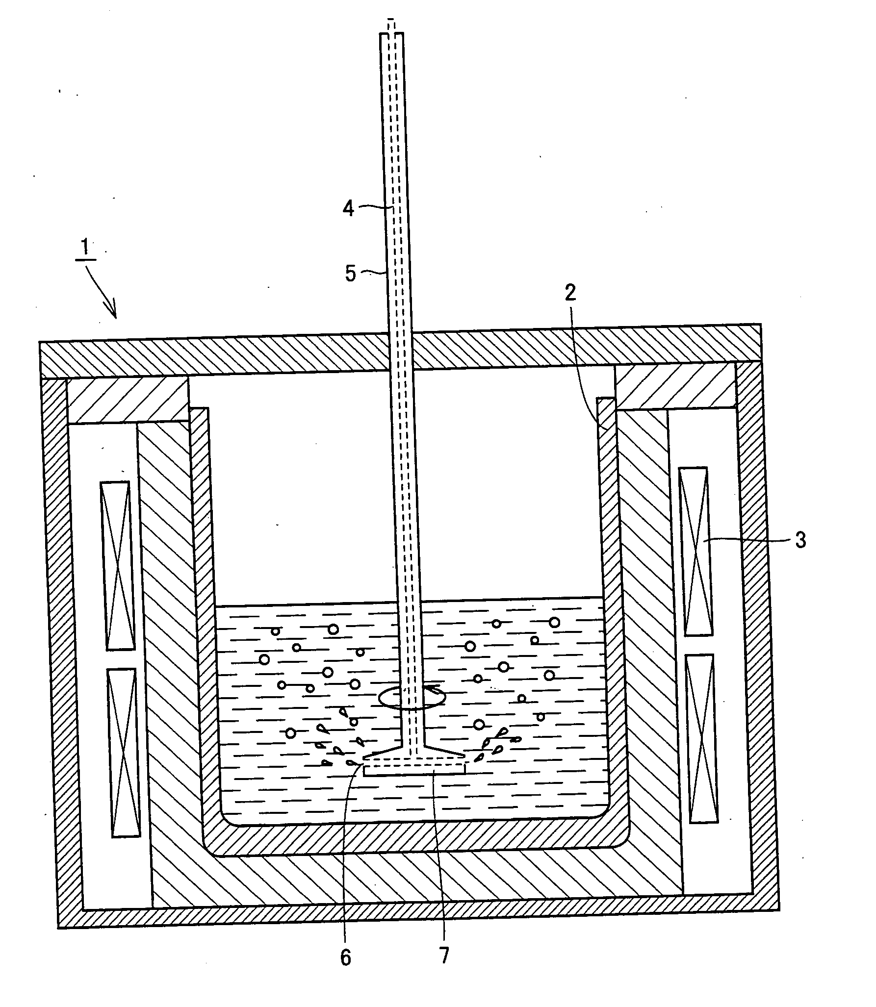
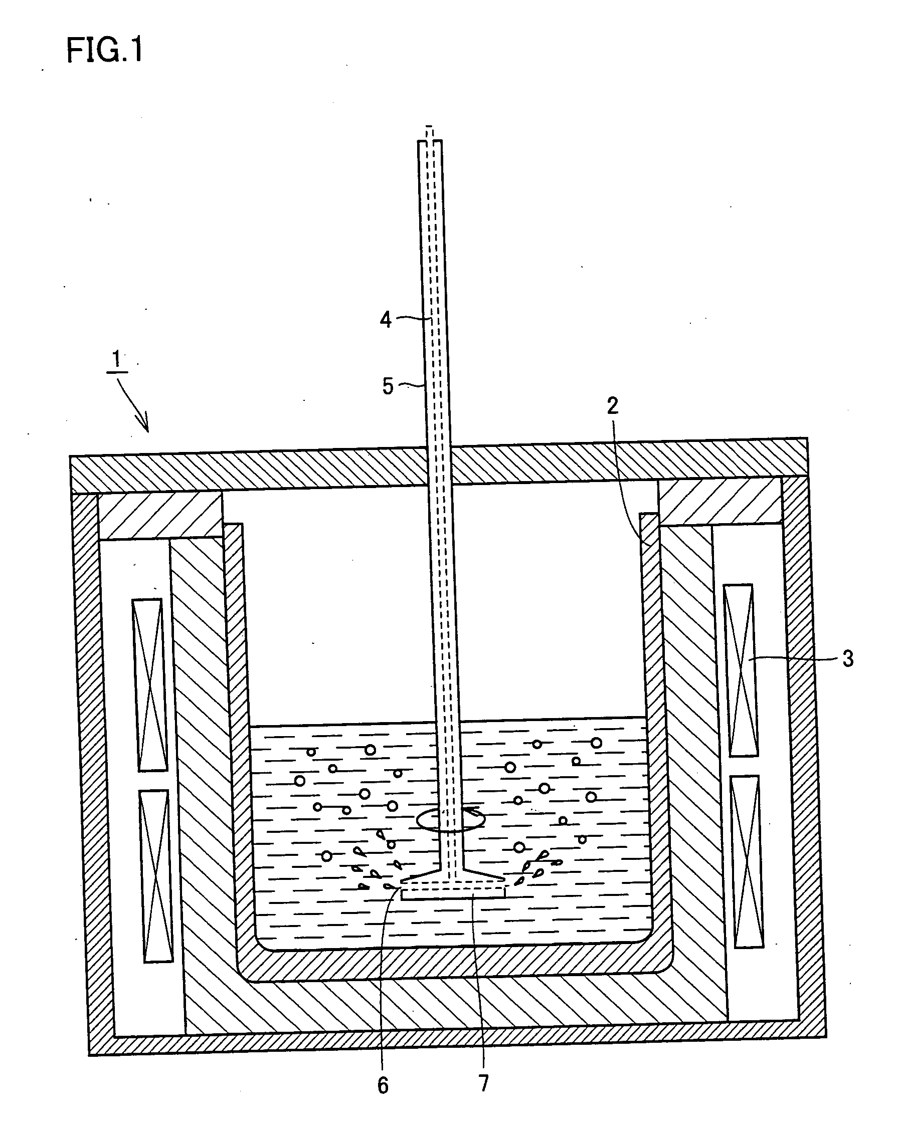
[0017] The principal object of the present invention is to provide a method of purifying an impurity element contained in metal such as silicon extremely efficiently through a low-priced process. In order to attain this object, a method of purifying silicon according to the present invention is characterized in holding silicon containing an impurity and a slag containing at least 45 percent by mass of SiO2 in a molten state, blowing gas introduced for refining reaction containing at least one selected from a group consisting of water vapor, oxygen gas, oxygen-containing gas and halogen-based gas into the molten silicon and stirring the same.

Problems solved by technology

If the oxide or the like is merely reduced, however, the quantities of impurities other than the desired simple metallic element are generally improper, and the quantities of the impurities are adjusted, mostly reduced in general.
In order to satisfy requirements for application to the electronic device, extremely complicated fabrication steps and strict fabrication step management are required and hence the fabrication cost therefor must inevitably be increased.
However, it is known that these elements have extremely large segregation coefficients of about 0.35 and 0.8 respectively and hence purification utilizing solidification / segregation represented by the aforementioned unidirectional solidification is substantially ineffective.
While the aforementioned methods can be listed in relation to purification of silicon through a metallurgical procedure, none of these methods is commercially valid under the present circumstances due to the problem of the cost.
Referring to boron removal, the method of applying a plasma to the surface of molten silicon disclosed in Japanese Patent No. 3205352 or the method of immersing a torch in molten silicon disclosed in U.S. Pat. No. 5,972,107 has such a problem that a reaction site is so local that the obtainable throughput is limited and a device itself requires a high cost.
As to the method of stirring a molten bath of silicon with a rotating turbine wheel or through Lorenz force for blowing gas introduced for refining reaction such as argon containing water vapor thereinto disclosed in Japanese Patent Laying-Open No. 2001-58811, reduction of a device cost can be expected due to a simple device, while the reaction rate is not remarkably improved and there is still little prospect of commercialization.

Method used


Image

  • Silicon purifying method, slag for purifying silicon and purified silicon
  • Silicon purifying method, slag for purifying silicon and purified silicon

Examples


reference example 1

[0047] In this Example, a substance obtained by mixing silicon oxide powder and calcium oxide powder at a weight ratio of 65:35 was used as a slag material. Then, 1 kg of a substance obtained by blending raw silicon having a boron concentration adjusted to 7 ppm and the slag material with each other at a weight ratio of 4:1 was charged into the crucible 2. The smelting furnace 1 was set to an argon gas atmosphere of 1 atm, and the crucible 2 was thereafter heated with the electromagnetic induction heater 3 thereby melting the raw silicon and the slag material, which in turn were thereafter held at 1550° C.

[0048] The molten slag, having large specific gravity with respect to the molten silicon, precipitated on the bottom of the crucible 2. The shaft 5 was moved down through the hoist mechanism until the injection nozzle 7 of the stirring part 6 reached the portion around the interface between the molten slag and the molten silicon. When the shaft 5 was rotated at 400 rpm without gas...

reference example 2

[0049] Treatment was performed for two hours under conditions similar to those for Reference Example 1 except that the shaft 5 was rotated at 400 rpm while injecting argon gas from the injection nozzle 7 of the stirring part 6 at a flow velocity of 1 L / min. When the boron content was measured around the treatment, that before the treatment was 7.4 ppm and that after the treatment was 1.3 ppm.

example 1

[0050] Treatment was performed for two hours under conditions similar to those for Reference Example 1 except that the shaft 5 was rotated at 400 rpm while injecting gas introduced for refining reaction prepared by setting a water vapor content in argon gas to 30% from the injection nozzle 7 of the stirring part 6 at a flow velocity of 1 L / min. When the boron content was measured around the treatment, that before the treatment was 7.4 ppm and that after the treatment was 0.8 ppm.


PUM


Abstract

Method capable of preparing silicon having purity of about 6N applied to a solar cell efficiently at a low cost. Raw silicon containing boron and a slag are melted and a shaft is rotated by a rotating / driving mechanism for stirring the molten silicon. The molten slag is dispersed in the molten silicon, thereby accelerating the boron removal reaction. It is further effective to use a slag containing at least 45 percent by mass of silicon oxide or to blow gas mixed with water vapor into the molten silicon for refining reaction.

Description

TECHNICAL FIELD [0001] The present invention generally relates to a method of purifying silicon, and more specifically, it relates to a method of preparing a silicon material for a solar cell. BACKGROUND ART [0002] In general, a metallic element such as iron, aluminum, copper or silicon is extremely rarely present solely in nature, and most part thereof is present as a compound such as an oxide. In order to apply such a metallic element to a structural material, a conductive material or a semiconductor material, therefore, it is generally necessary to reduce an oxide or the like into the form of a simple metallic element. [0003] If the oxide or the like is merely reduced, however, the quantities of impurities other than the desired simple metallic element are generally improper, and the quantities of the impurities are adjusted, mostly reduced in general. Such a step of reducing the quantities of impurities is referred to as purification. [0004] The term purification denotes an oper...

Claims


Application Information

Patent Timeline
IPC IPC(8): C01B33/037
CPCC01B33/037
Inventor FUJIWARA, HIROYASUOTSUKA, RYOTATSUWADA, KENJIFUKUYAMA, TOSHIAKI
Owner SHARP KK
Learn More