
Patterned wafer inspection method and apparatus therefor
a technology of patterned wafers and inspection methods, applied in semiconductor/solid-state device testing/measurement, material analysis using wave/particle radiation, instruments, etc., can solve the problems of reducing the detection reducing the inspection speed or yield of inspection, and reducing the number of pixels. , the defect detection process can be simplified, and the improvement of the inspection speed or yield is limited
- Summary
- Abstract
- Description
- Claims
- Application Information
AI Technical Summary
Benefits of technology
Problems solved by technology
Method used
Image

Examples
embodiment 1
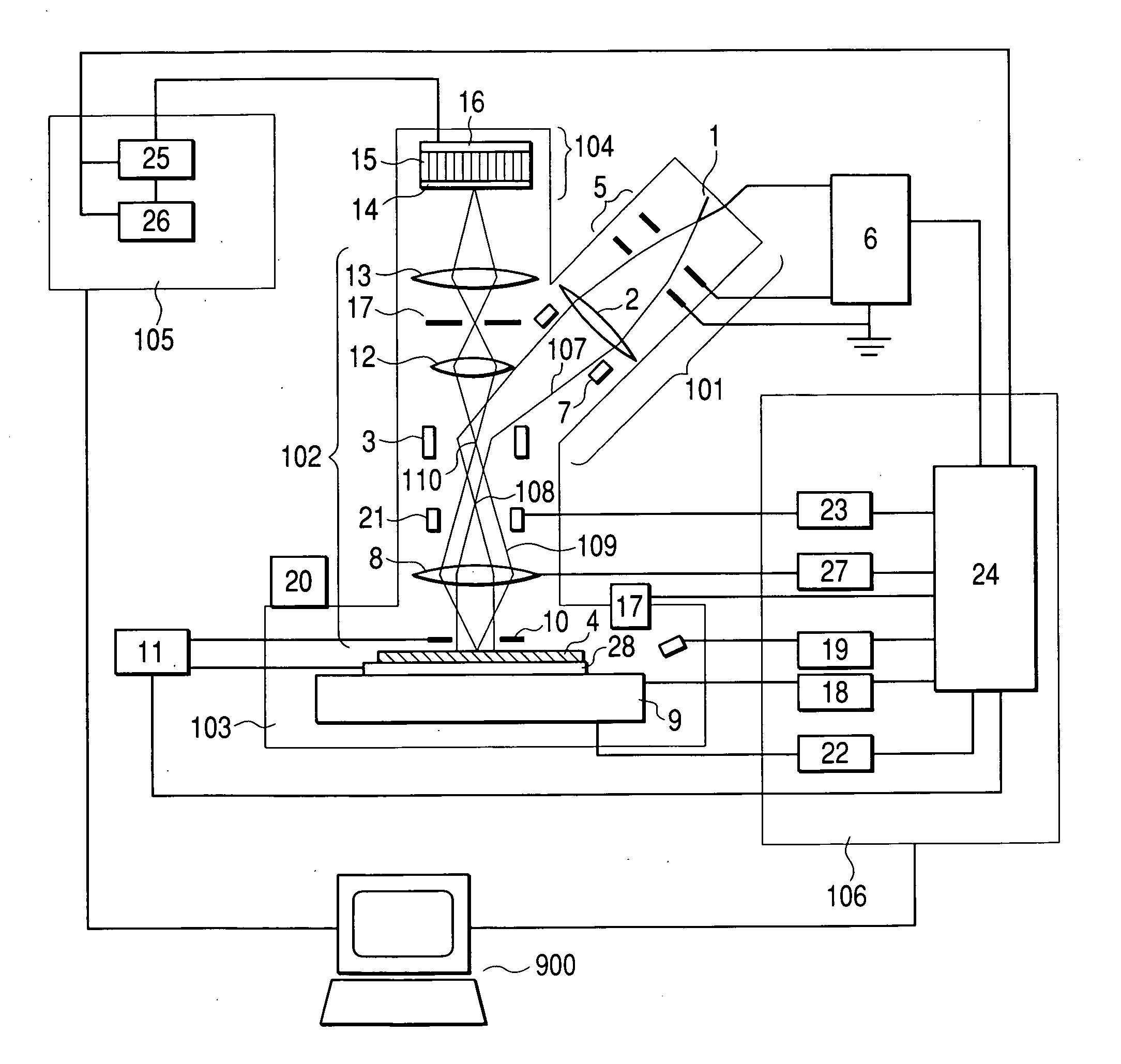
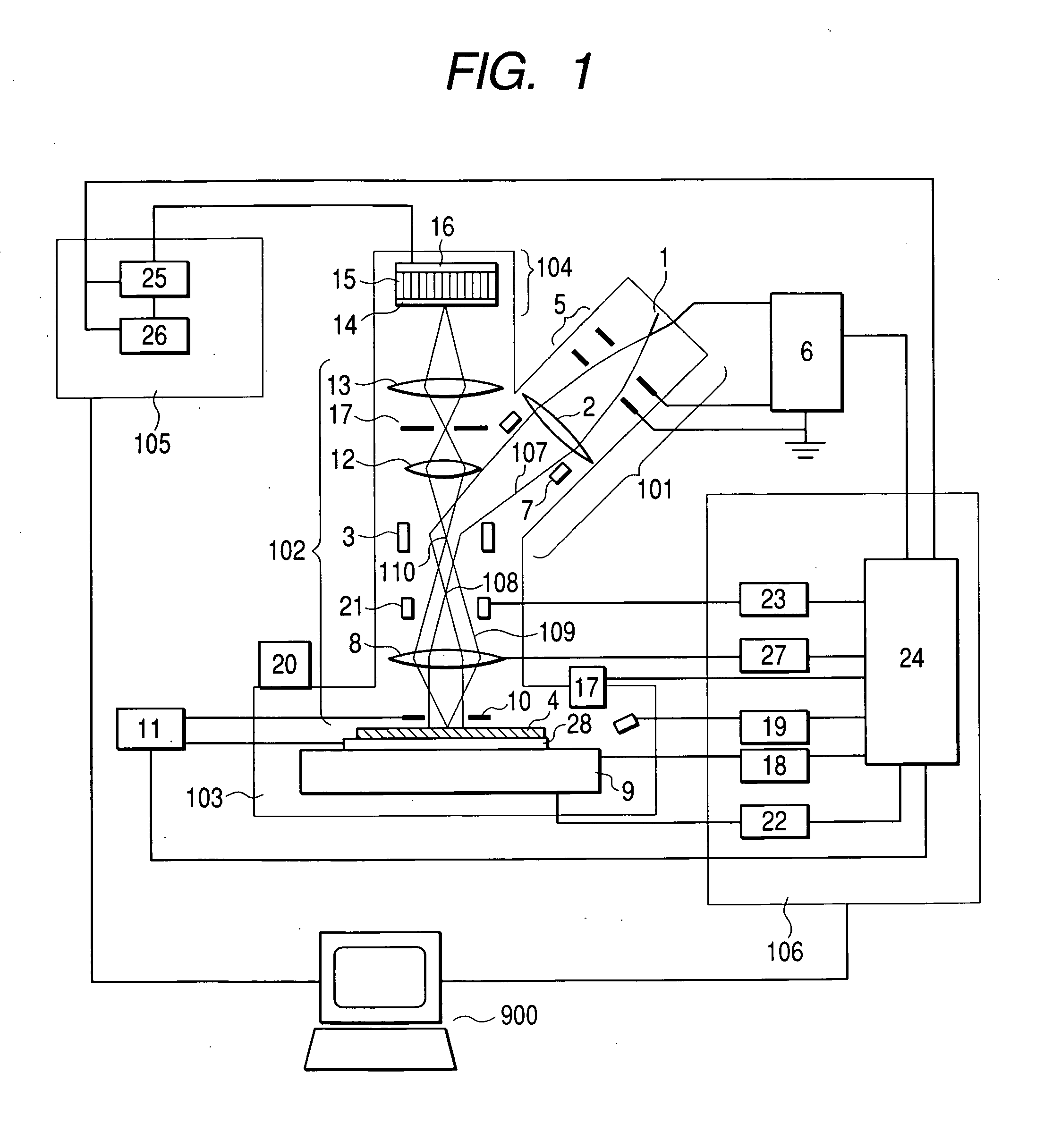
[0028] In the present embodiment, a description will be given to an example in which the present invention is applied to a defect inspection apparatus of a mirror projection (MPJ) type. The description will be given first to the principle of the MPJ and a problem to be solved.
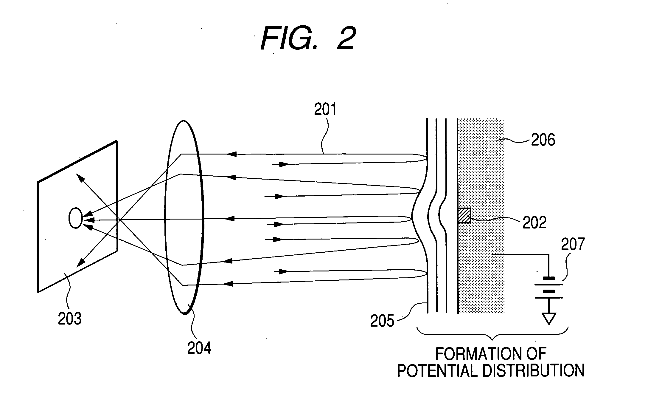
[0029] A consideration will be given to a situation in which the plurality of target regions (areal regions) of a surface of a sample are irradiated with a planar electron beam having a two-dimensional expansion and a negative potential is further applied to a wafer. The negative potential is adjusted to such a value as to return a major part of the electron beam in the vicinity of the outermost surface of the wafer. Specifically, the negative potential is adjusted to a level higher by 0.5 V to 5 V than a potential at an electron source. At this time, the irradiation beam is reflected immediately before the sample and returned by an electric field without colliding with the sample. The electrons will be termed...
embodiment 2
[0062] In the first embodiment, the lowest permissible positional accuracy of defect detection has been suppressed to about triple the pattern size or less. To simply detect only the presence or absence of a defect, however, the present invention can be implemented with a simpler structure. In the present invention, what is obtainable as an image is a potential distribution distorted by a defect. Accordingly, there is no image in a normal portion and an image signal is intensified only in a defective portion. If the accuracy required of the location of a defect is not so high, the presence or absence of a defect can be monitored based on the intensity of a whole image instead of obtaining a 2-D intensity distribution of an image.
[0063] In the present embodiment, the size of the irradiated region for one shot is adjusted to about 5 μm and mirror electrons are signalized by using a simple detector for measuring only the magnitude of the intensity of a whole signal. The large differen...
embodiment 3
[0068] The present embodiment shows an example in which a second SEM tube 801 and the like are provided to enable a detailed defect inspection. FIG. 8 shows a structure thereof. Although the structure shown in the drawing is obtained by adding the SEM tube and the like to the first embodiment, the second embodiment may also be used instead of the first embodiment.
[0069] When particularly detailed observation should be performed with respect to a wafer on which the location of a defect has been determined according to the first embodiment (or the second embodiment), the wafer is transferred to the sample stage 37 under the SEM tube 801 by using a wafer transfer mechanism 36. The wafer transfer mechanism 36 comprises a mechanism capable of transferring the wafer from the sample room 103 to a sample room 802 without bringing the wafer out of the vacuum ambience. In the SEM tube 801, an electron beam 803 emitted from the electron gun 38 forms an extremely small spot on a transferred sa...
PUM
| Property | Measurement | Unit |
|---|---|---|
| area | aaaaa | aaaaa |
| energy distribution | aaaaa | aaaaa |
| voltage | aaaaa | aaaaa |
Abstract
Description
Claims
Application Information