

Ceramic thin film on various substrates, and process for producing same
a technology of ceramic thin film and substrate, applied in the field of thin film, can solve the problems of limited sic production rate, increased disorder of sic network, shrinking and outgasing phenomena,
- Summary
- Abstract
- Description
- Claims
- Application Information
AI Technical Summary
Problems solved by technology
Method used
Image

Examples
example 1
Synthesis of an n-Type Amorphous Silicon Carbide (N-Doped) Thin Film Via the PS-CVD Process
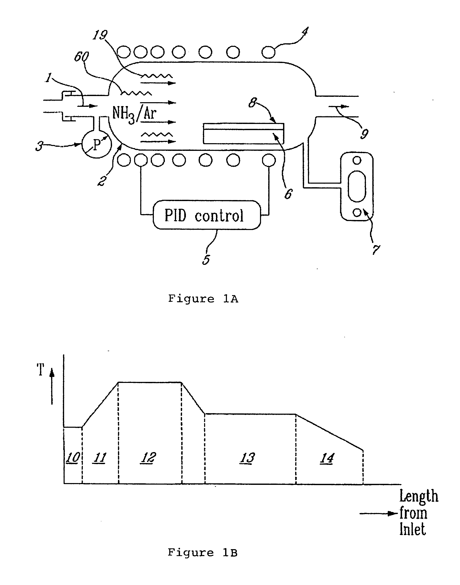
[0112] Synthesis—Charges of polydimethylsilane and in-house prepared polymethylsilane (M. Scarlete et al., 1995, Chem. Mater., 6, p. 1214) have been pyrolyzed in a single-zone Lindberg ceramic furnace. The synthesis was performed in a 2″ quartz tube attached to a silicone-based hydraulic lock bubbler and to a vacuum line capable of providing a reduced pressure of 5*10−2 torr. The synthesis was performed in a gaseous atmosphere of UHP—Ar or in home purified NH3. The purification of NH3 was obtained via passing the gas through a 1000 mm column of KOH and a 250 mm column of a mixture of 3 and 4 Å molecular sieves. The furnace was operated via a PID Eurotherm temperature-controller proving ±0.5° C. in the range of 110 to 1100° C. at 10 torr above the atmospheric pressure. The atmosphere of the pyrolysis was carefully purified from oxygen and water vapours via a series of evacuations / Ar-fillings. ...
example 2
Synthesis of a p-Type Amorphous Silicon Carbide (B-Doped) Thin Film Via the PS-CVD Process
[0127] Synthesis—Charges of poly(dimethylsilane) (PDMS) were pyrolyzed in a Lindberg* BlueM single-zone furnace. The furnace was operated via a PID Eurotherm temperature-controller providing an accuracy of ±0.5° C. in the ranger of 110 to 1100° C. The furnace was equipped with a 2.5″ quartz tube attached to a silicone-based hydraulic lock bubbler and a vacuum line capable of providing 5*10−2 torr vacuum as measured with a Welch Pirani-gauge. The atmosphere prior to pyrolysis was carefully purged of moisture and oxygen via a series of evacuations and UHP-Ar fillings. The residual oxygen level obtained after the purging procedure was measured using an Innovative Technology gauge and was found to be below 1 ppm. Once purged, a partial pressure of BCl3 was created in the reactor.
[0128] The substrates used were p-type (B doped) (100) oriented single crystal silicon substrates, electroni...
example 3
Synthesis of an Amorphous Silicon Carbonitride Thin Film Via the PS-CVD Process
[0133] Synthesis—In-house prepared polymethylsilane and poly(dimethyl)silane were pyrolyzed under NH3. The nitrogen-containing amorphous layers were deposited on electronic-grade substrates such as silicon single crystal wafers, quartz, and alumina. The pyrolyses were conducted at 5-20 torr above the atmospheric pressure and were undertaken in a Lindberg single-zone, programmable furnace equipped with a Eurotherm PID temperature controller with a maximum temperature of 1100±0.5° C. The temperature cycle during the PS-CVD process was the following: 4° / min 110-450° C., 30 min at 450° C., 4-8° C. / min up to 1050° C., and 30 min at 1050° C. (batch process).
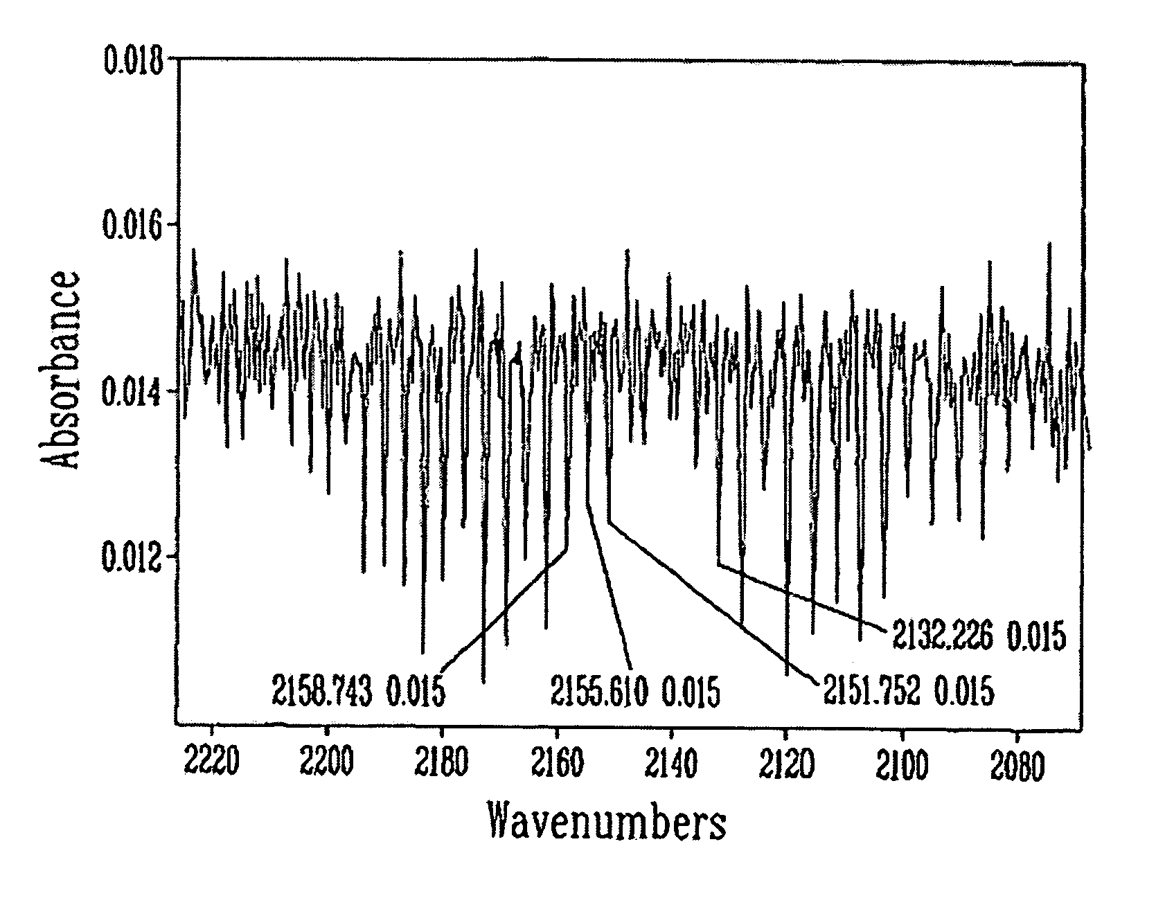
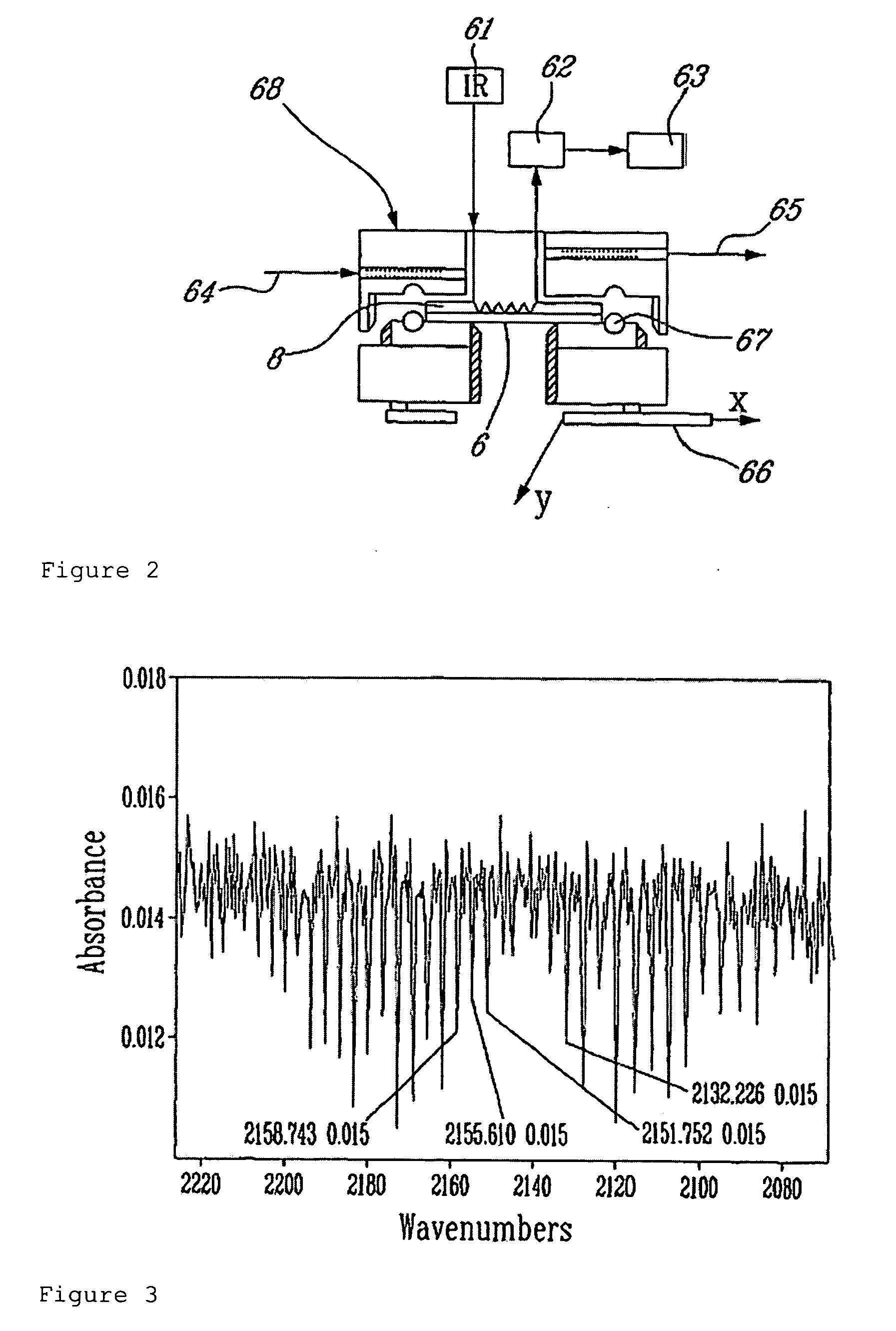
[0134] Characterization—Prior to analysis of the film, the products of the chemical reactions involving the carbon-for-nitrogen exchange were followed in the ceramic residue of the polymer. There was continuous C / N replacement activated by a critical tempe...
PUM
| Property | Measurement | Unit |
|---|---|---|
| Grain size | aaaaa | aaaaa |
| Grain size | aaaaa | aaaaa |
| Grain size | aaaaa | aaaaa |
Abstract
Description
Claims
Application Information