Structure and method for III-nitride device isolation

Active Publication Date: 2005-06-30
INFINEON TECH AMERICAS
View PDF3 Cites 5 Cited by
  • Summary
  • Abstract
  • Description
  • Claims
  • Application Information

AI Technical Summary

Benefits of technology

[0026] The large dielectric breakdown field in the III-nitride semiconductor material system permits the construction of power devices with reduced size standoff regions. The material system also permits the production of devices with reduced specific on resistance in comparison with known devices of similar voltage ratings. Due to the higher performance of the III-nitride semiconductor material, in a smaller size than traditional materials, device isolation takes on a greater importance. The device isolation provided according to the present invention can provide improved performance suitable for the III-nitride semiconductor materials, where such isolation was not needed or recognized in silicon semiconductors due to the lower electric fields generated by devices during ope

Problems solved by technology

A drawback of III-nitride devices that permit high current densities with low resistive losses is the limited thickness that can be achieved in the strained AlGaN/GaN system.
The difference in the lattice structures of these types of materials produces a strain that can result in dislocation of films grown to produce the different layers.
This results in high levels of leakage through a barrier layer such as an insulator, for example, and makes device isolation problematic.
However, these processes and structures are difficult to implement and are not commercially feasible.
However, no equivalent material to the native oxides in silicon is available for suitable dielectrics in the III-nitride material system.
Dielectric materials that would otherwise be suitable in silicon semiconductors, for example, do not transf

Method used


Image

  • Structure and method for III-nitride device isolation
  • Structure and method for III-nitride device isolation

Examples


Embodiment Construction

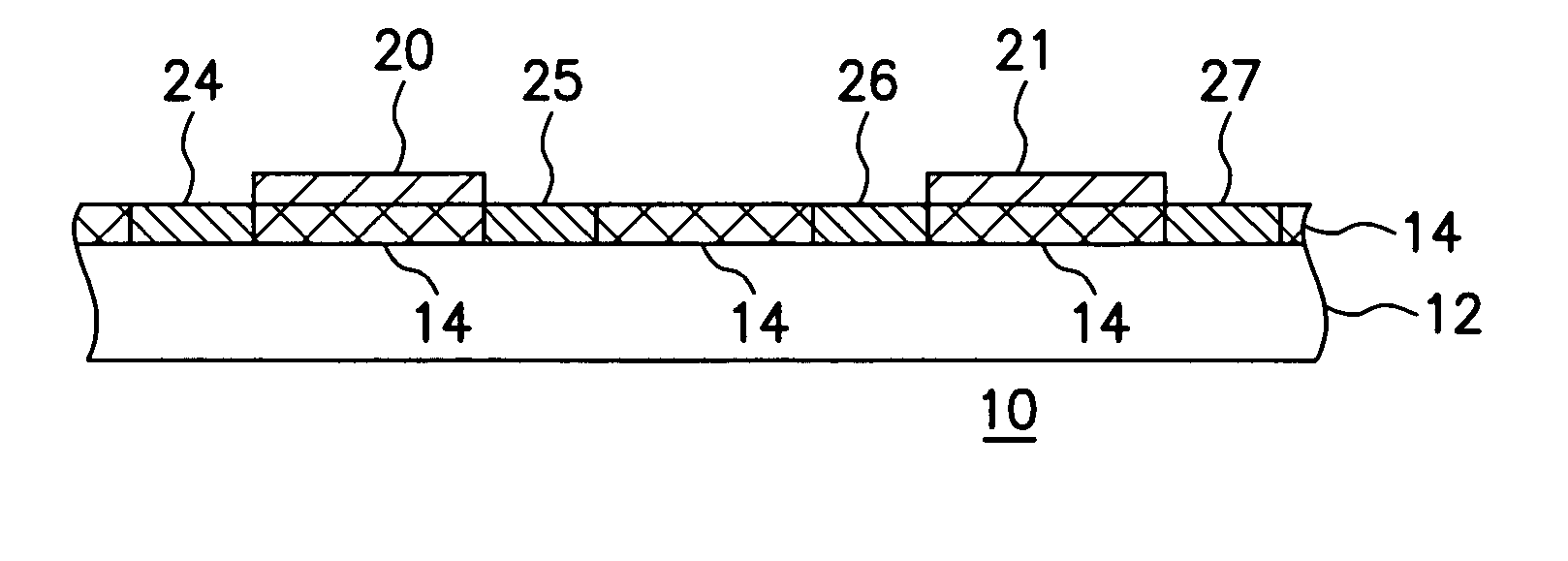
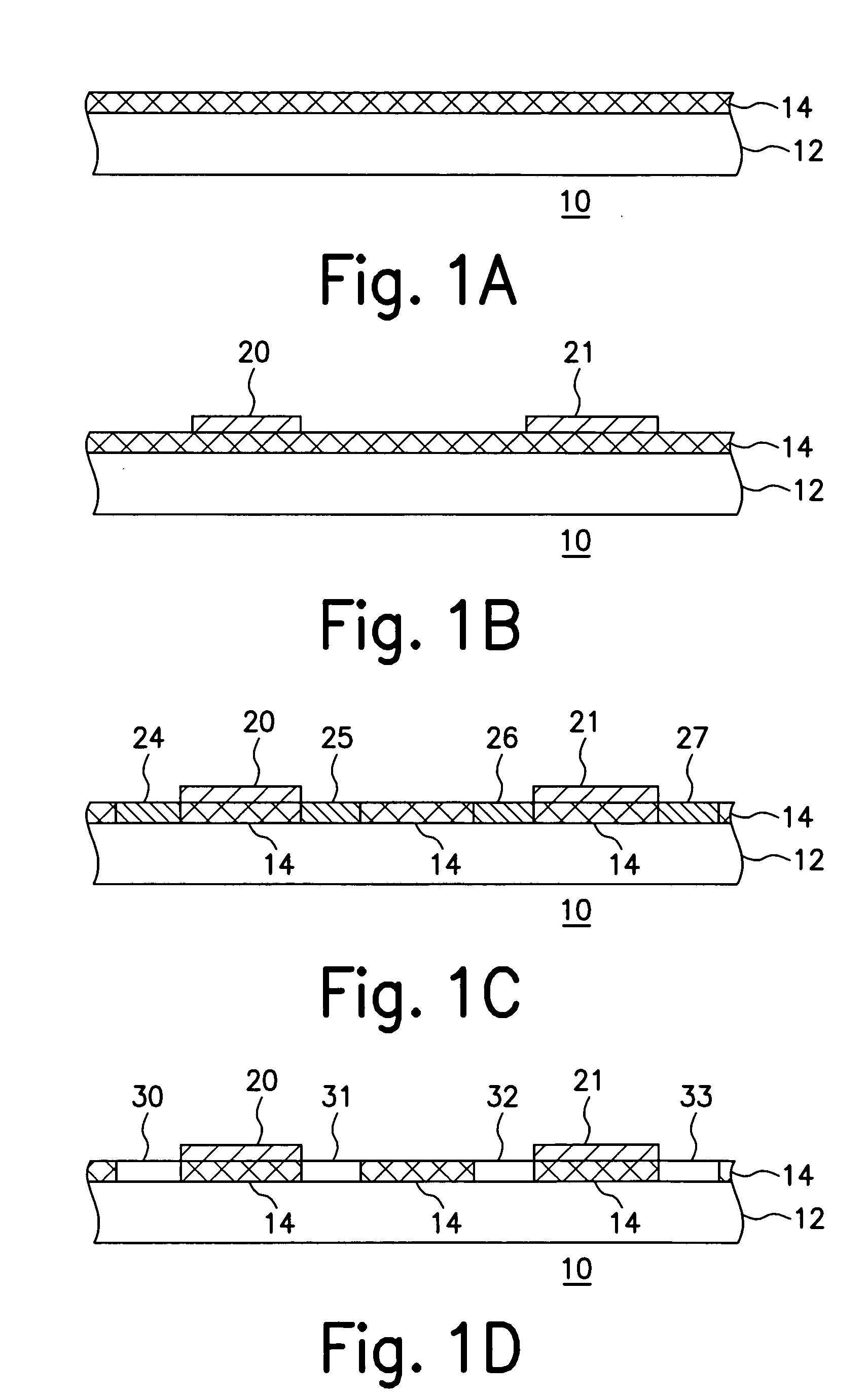
[0036] The advantages of III-nitride materials in conducting large amounts of current and withstanding high voltage are typically realized in a GaN / AlGaN layer construction, although other types of constructions may readily be used in the III-nitride material system. For example, whenever two different materials in the III-nitride material system have different in-plane lattice constants, such that a high mobility interface is formed between the two layers, the advantages of high blocking current and high current conduction in devices constructed with the interface are readily observed.

[0037] It is often the case that III-nitride material semiconductor devices are formed on a wafer level, where a number of devices may be fabricated at the same time. Accordingly, a substrate is often used as a base upon which the III-nitride semiconductor devices may be formed, where the devices are composed of a buffer layer and / or a body layer with different composition III-nitride materials. Ofte...


PUM


Abstract

Isolation of III-nitride devices may be performed with a dopant selective etch that provides a smooth profile with little crystal damage in comparison to previously used isolation techniques. The dopant selective etch may be an electro-chemical or photo-electro-chemical etch. The desired isolation area may be identified by changing the conductivity type of the semiconductor material to be etched. The etch process can remove a conductive layer to isolate a device atop the conductive layer. The etch process can be self stopping, where the process automatically terminates when the selectively doped semiconductor material is removed.

Description

RELATED APPLICATION [0001] The present application is based on and claims benefit of U.S. Provisional Application No. 60 / 527,635, filed Dec. 5, 2003, entitled Electro-Chemical Etch for Device Isolation in III-Nitride Devices to which a claim of priority is hereby made, and the disclosure of which is hereby incorporated herein by reference.BACKGROUND OF THE INVENTION [0002] 1. Field of the Invention [0003] The present invention relates generally to an isolation technique for III-nitride devices, and relates more particularly to a device and method for an electrochemical etch to produce device isolation in III-nitride semiconductor devices. [0004] 2. Description of Related Art [0005] III-nitride semiconductors are presently known that exhibit a large dielectric breakdown field of greater than 2.2 MV / cm. III-nitride heterojunction structures are also capable of carrying extremely high currents, which makes devices fabricated in the III-nitride material system excellent for power applic...

Claims


Application Information

Patent Timeline
IPC IPC(8): H01LH01L21/76H01L21/762H01L29/00
CPCH01L21/7605H01L21/764H01L21/76224
Inventor BRIDGER, PAUL
Owner INFINEON TECH AMERICAS
Why Eureka
Try Eureka