Method for manufacturing semiconductor device

Inactive Publication Date: 2005-06-30
DONGBU ELECTRONICS CO LTD
View PDF17 Cites 16 Cited by
  • Summary
  • Abstract
  • Description
  • Claims
  • Application Information

AI Technical Summary

Benefits of technology

[0016] Accordingly, the present invention has been made to solve the above-mentioned problems, and an object of the present invention is to provide a method for manufacturing a

Problems solved by technology

The narrowing of the interconnect generally causes an increase of resistance in the interconnect and furthermore a delay of signal transfer.
However, in the multi-layered interconnect structure, an interval (or spacing) between adjacent interconnect lines is further narrowed so that parasitic capacitance between interconnects on the same layer increases and signal transfer delay of the semiconductor device further increases.
However, in case of copper, since vapor pressure of certain etching by-products is low, it is generally difficult to dry

Method used


Image

  • Method for manufacturing semiconductor device
  • Method for manufacturing semiconductor device
  • Method for manufacturing semiconductor device

Examples


Embodiment Construction

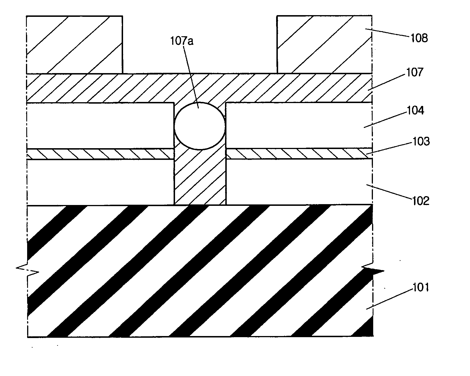
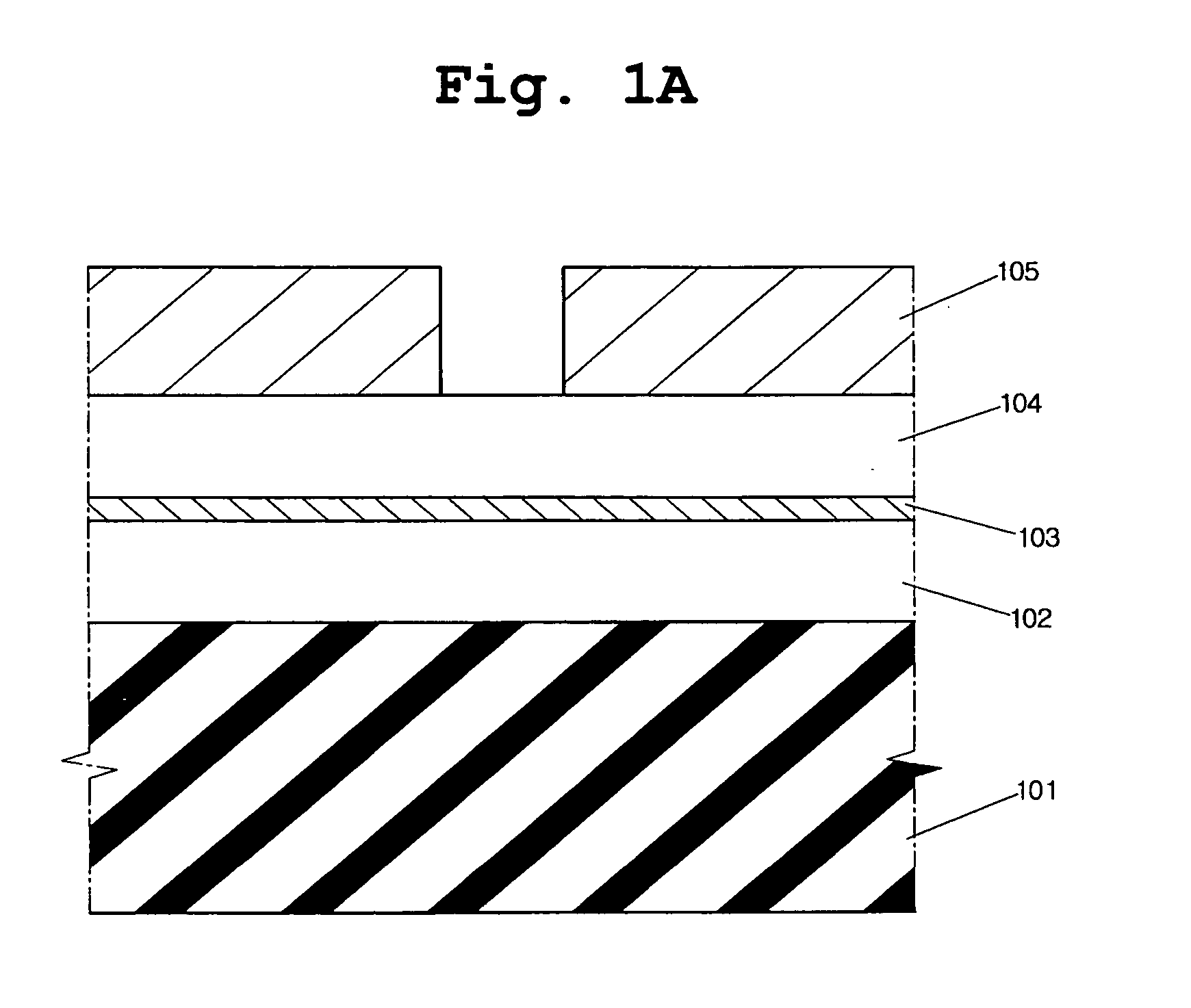
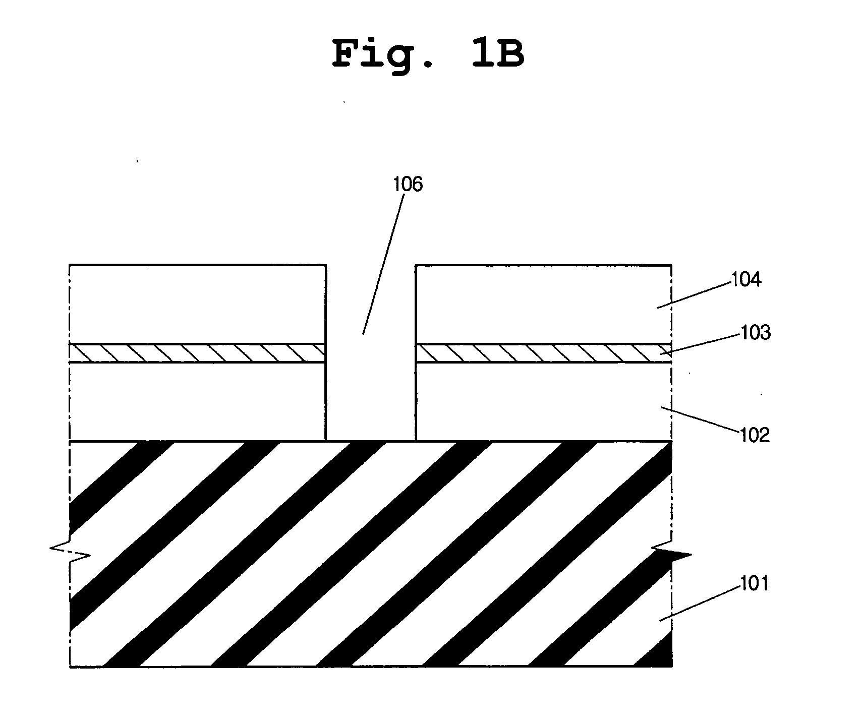
[0030] Hereinafter, a preferred embodiment of the present invention will be described with reference to the accompanying drawings. FIGS. 2A to 2F are cross-sectional views showing a method for manufacturing a semiconductor device according to a preferred embodiment of the present invention.

[0031] First, as shown in FIG. 2A, a first interlayer dielectric 202 with low permittivity is deposited on a semiconductor substrate 201. Herein, although not shown in the drawing, it is evident that on the semiconductor substrate, an isolation layer defining an active region of the substrate 201, a capacitor and / or a transistor on the active region, etc. may be previously formed.

[0032] The first interlayer dielectric 202 can be formed of various materials. In particular, a tetraethyl orthosilicate (TEOS)-based oxide layer (such as Low Pressure-TEOS, O3-TEOS, d-TEOS and so on), undoped silicate glass (USG), fluorosilicate glass (FSG), SiH4-based glass layer (e.g., deposited by High Density Plasm...


PUM

PropertyMeasurementUnit
Temperatureaaaaaaaaaa
Thicknessaaaaaaaaaa

Abstract

A method for manufacturing a semiconductor device which, on performing a via first Dual Damascene process, inhibits or prevents the formation of a void in a bottom anti-reflective coating filling a via hole. The method typically includes the steps of forming a bottom anti-reflective coating (BARC) in a via hole in an interlayer dielectric on a semiconductor substrate sufficiently to fill the via hole; disposing an acid diffusion material on the BARC; forming a cross-link layer between the BARC and the acid diffusion material; removing the remaining acid diffusion material; and etching the cross-link layer, the BARC and the interlayer dielectric to form a trench extending from an upper portion of the via hole.

Description

BACKGROUND OF THE INVENTION [0001] 1. Field of the Invention [0002] The present invention relates to a method for manufacturing a semiconductor device, and more particularly to a semiconductor device and method for manufacturing a semiconductor device which, on performing a “via first” Dual Damascene process, inhibits or prevents the formation of a void in a bottom anti-reflective coating filling a via hole. [0003] 2. Description of the Background [0004] Generally, with the high integration of semiconductor devices, an interconnect becomes narrowed. The narrowing of the interconnect generally causes an increase of resistance in the interconnect and furthermore a delay of signal transfer. To solve the problem of signal transfer delay, a multi-layered interconnect structure has been introduced, generally replacing the previous single layered interconnect structure. [0005] However, in the multi-layered interconnect structure, an interval (or spacing) between adjacent interconnect lines...

Claims


Application Information

Patent Timeline
IPC IPC(8): G03F7/16H01L21/4763H01L21/768H01L23/48H01L23/52H01L29/40
CPCY10S430/108H01L21/76808G03F7/16
Inventor CHOI, YONG JUN
Owner DONGBU ELECTRONICS CO LTD
Why Eureka
Try Eureka