Dual step source/drain extension junction anneal to reduce the junction depth: multiple-pulse low energy laser anneal coupled with rapid thermal anneal

a junction depth and annealing technology, applied in the field of forming mos transistors with reduced junction depth, can solve the problems of gate shape distortion, pulse laser annealing in combination with pai, difficult to obtain highly steep ultra-shallow junction profiles, etc., and achieve the effect of reducing the junction sheet resistan

Inactive Publication Date: 2005-07-21
CHARTERED SEMICONDUCTOR MANUFACTURING
View PDF8 Cites 25 Cited by
  • Summary
  • Abstract
  • Description
  • Claims
  • Application Information

AI Technical Summary

Benefits of technology

[0013] Another objective of the invention is to describe a dual-step annealing method that uses multiple-pulse low energy laser anneal followed by rapid thermal anneal.
[0014] In accordance with these objectives, a process is described to form a MOSFET device with shallow junction in the source/drain extension regions. After forming a MOSFET device up to and including the step of forming the gate structure but before the formation of sidewall dielectric spacers, a pre-amorphizing implant (PAI) is performed with Si+ or Ge+ ions to form a thin PAI layer o

Problems solved by technology

With the conventional junction formation by ion implant and rapid thermal anneal, it is very difficult to obtain highly steep ultra-shallow junction profiles because the interaction between implantation induced point defects and dopant atoms during annealing can considerably broaden the profile shape through the mechanism of transient enhanced diffusion (TED).
However, the method has integration issues related to ga

Method used


Image

  • Dual step source/drain extension junction anneal to reduce the junction depth: multiple-pulse low energy laser anneal coupled with rapid thermal anneal
  • Dual step source/drain extension junction anneal to reduce the junction depth: multiple-pulse low energy laser anneal coupled with rapid thermal anneal
  • Dual step source/drain extension junction anneal to reduce the junction depth: multiple-pulse low energy laser anneal coupled with rapid thermal anneal

Examples


Embodiment Construction

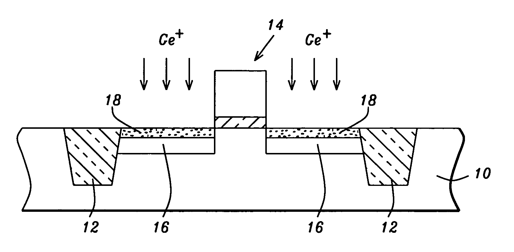
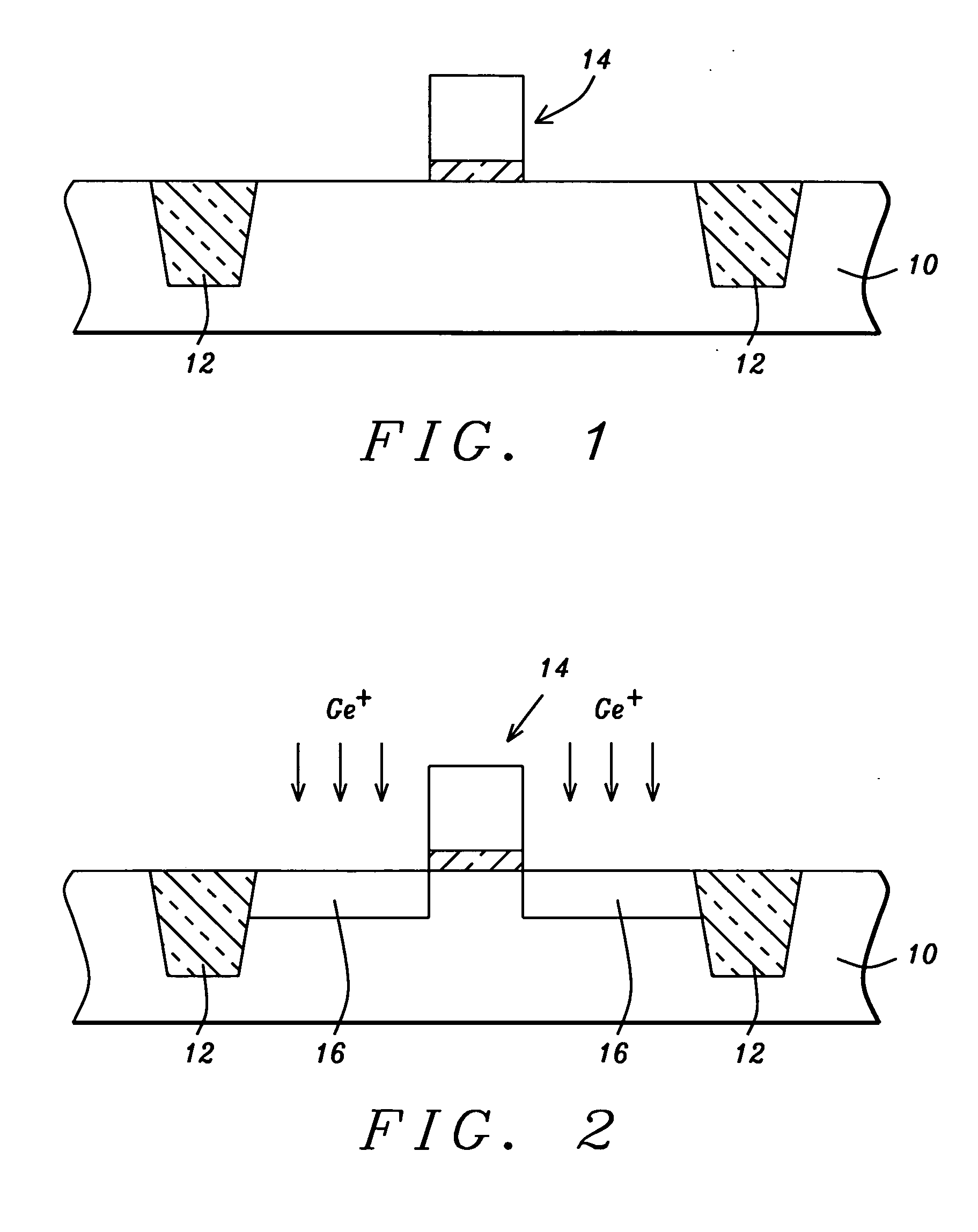
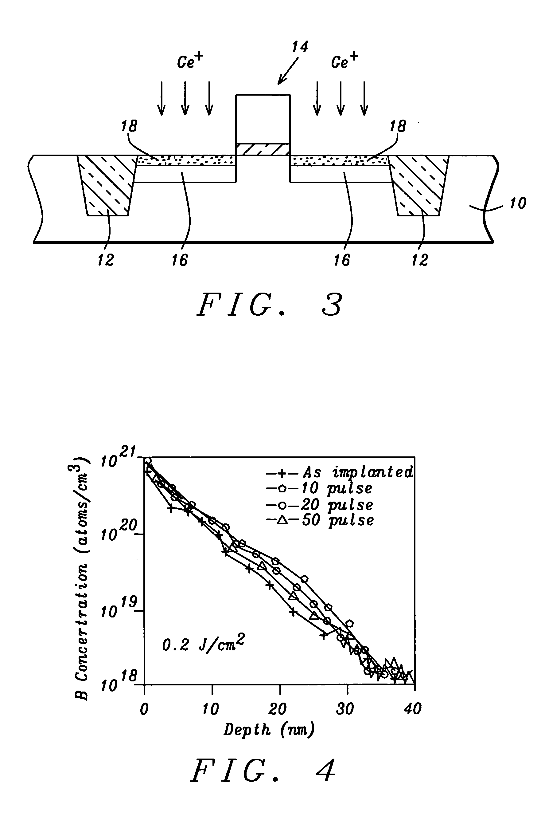
[0022] Using the standard processes from prior art, a field effect transistor device is formed in a silicon semiconductor substrate 10, n type silicon in this embodiment, as shown in FIG. 1 up to and including the steps of forming shallow trench isolations (STI) 12 and the gate electrode structure 14.

[0023] A pre-amorphizing Ge+ ion implant known in prior art is performed to form a thin PAI layer 16 in silicon as shown in FIG. 2. The implant conditions are: ion energy of approximately 1 to 20 keV and dose of about 1E14 to 1E16 ion / cm2. The PAI layer thickness is approximately between about 2 and 40 nm. Heavy Ge+ ions cause adequate damage to the crystalline silicon lattice thereby rendering the top surface amorphous. Since the melting point of amorphous silicon layer is approximately 300 C less than that of crystalline silicon, selective annealing process is therefore enabled. It is to be noted the lattice damage during this step is later repaired during subsequent annealing steps...


PUM


Abstract

A process is described to form a semiconductor device such as MOSFET or CMOS with shallow junctions in the source/drain extension regions. After forming the shallow trench isolations and the gate stack, sidewall dielectric spacers are removed. A pre-amorphizing implant (PAI) is performed with Ge+ or Si+ ions to form a thin PAI layer on the surface of the silicon regions adjacent to the gate stack. B+ ion implantation is then performed to form source/drain extension (SDE) regions. The B+ implant step is then followed by multiple-pulsed 248 nm KrF excimer laser anneal with pulse duration of 23 ns. This step is to reduce the sheet resistance of the junction through the activation of the boron dopant in the SDE junctions. Laser anneal is then followed by rapid thermal anneal (RTA) to repair the residual damage and also to induce out-diffusion of the boron to yield shallower junctions than the just-implanted junctions prior to RTA.

Description

BACKGROUND OF THE INVENTION [0001] (1) Field of the Invention [0002] The present invention relates generally to a method of forming a semiconductor device, and more particularly to form an MOS transistor with reduced junction depth using a combination of multiple-pulsed laser anneal and rapid thermal anneal. [0003] (2) Description of the Prior Art [0004] Ion implantation process is essential to fabricate modern integrated circuits. Doping or otherwise modifying silicon or other semiconductor wafers relies on this technology, which involves generating the required beam of ions and implanting them into the substrate so that they come to rest just below the semiconductor surface. Most commonly implanted species are: antimony, arsenic, boron, boron difluoride, germanium, and phosphorous. Currently, ion implantation is used to form source and drain regions, shallow extension junctions between the channel and source / drain contacts, and electrically active poly-silicon gate electrodes. Ion...

Claims


Application Information

Patent Timeline
IPC IPC(8): H01L21/265H01L21/268H01L21/324
CPCH01L21/26506H01L21/26513H01L21/823418H01L21/324H01L21/268
Inventor POON, CHYIU HYIATAN, LENG SEOWCHO, BYUNG JINSEE, ALEXBHAT, MOUSUMI
Owner CHARTERED SEMICONDUCTOR MANUFACTURING
Why Eureka
Try Eureka