Semiconductor device and manufacturing method thereof

a technology of semiconductors and manufacturing methods, applied in the direction of photoelectric discharge tubes, radio-controlled devices, instruments, etc., can solve the problems of parts not being fixed firmly, parts may not be fixed firmly any more, and the stress is not relaxed enough, so as to reduce the volume of parts, reduce the cost, and reduce the noise superposition

Inactive Publication Date: 2005-08-04
SEMICON ENERGY LAB CO LTD
View PDF93 Cites 88 Cited by
  • Summary
  • Abstract
  • Description
  • Claims
  • Application Information

AI Technical Summary

Benefits of technology

[0050] By integrally forming a visible light sensor and an amplifier circuit including a TFT over a same substrate, it is possible to reduce the cost, to decrease the volume of the parts because it can be made thinner, to miniaturize the area where the parts are mounted, and to reduce the superposition of the noise.
[0051] When the visible light sensor is formed using the amorphous silicon film, the infrared light cut filter is no longer necessary, and the visible light sensor with the variation in the output value reduced between the visible light sensors can be obtained. In addition, the amplifier circuit including the TFT formed over the same substrate makes it possible to increase th

Problems solved by technology

Therefore, when the parts are mounted by soldering for example, it is difficult to keep the parts fixed firmly.
In the case where the region in which the parts are fixed is small and where the degree of hardness of the sensor element (which means the mechanical strength of the single-crystal silicon substrate or the glass substrate) is high, when th

Method used


Image

  • Semiconductor device and manufacturing method thereof
  • Semiconductor device and manufacturing method thereof
  • Semiconductor device and manufacturing method thereof

Examples


embodiment 1

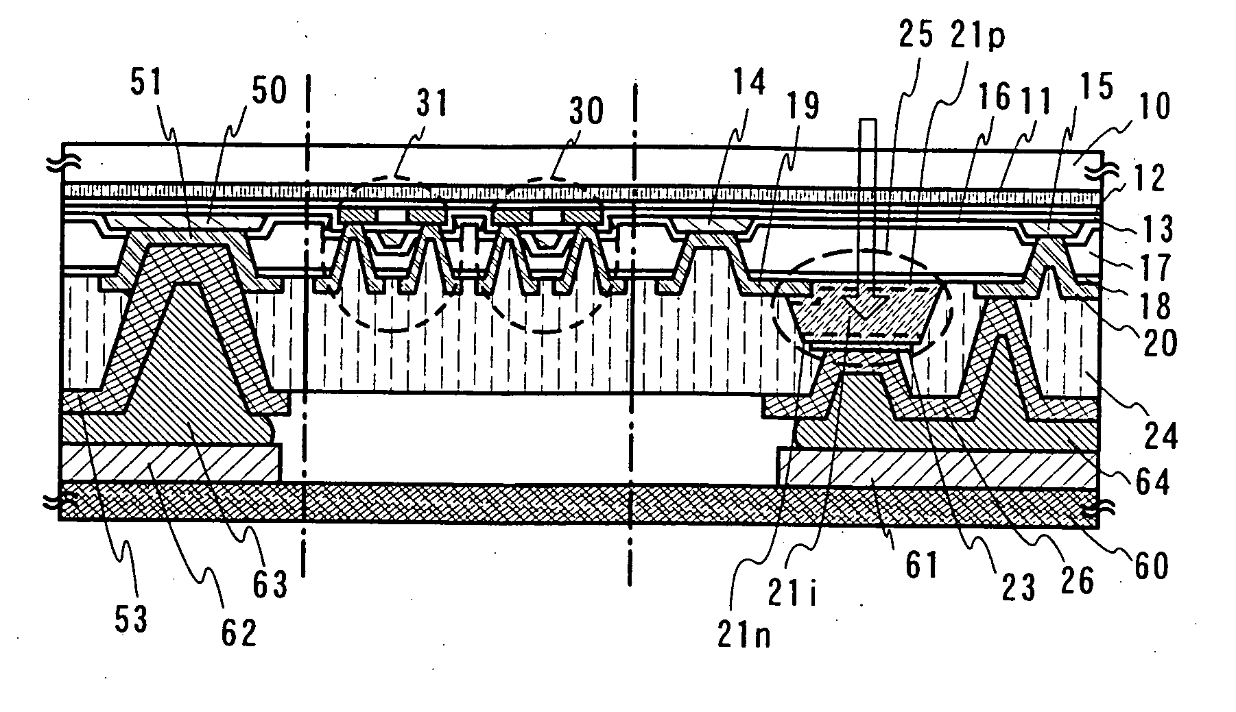
[0132] This embodiment explains a manufacturing process that is partially different from that shown in the embodiment mode with reference to FIGS. 7A and 7B. It is noted that the same reference numeral as that in FIGS. 1A to 3C is given to the same part in FIGS. 7A and 7B except for the second electrode.

[0133] Initially, the processes up to forming the photoelectric conversion layer and forming the metal film to become the second electrode afterward are performed according to the embodiment mode.

[0134] In order to decrease the number of masks and processes, in this embodiment, after forming a second electrode 723 made of Ti, etching gas is changed, and the photoelectric conversion layer including the amorphous silicon film is etched in a self-aligning manner using a resist mask 722 used for forming the second electrode 723. The cross-sectional view of this process is shown in FIG. 7A.

[0135] When the photoelectric conversion layer is patterned, since the top surface of the first e...

embodiment 2

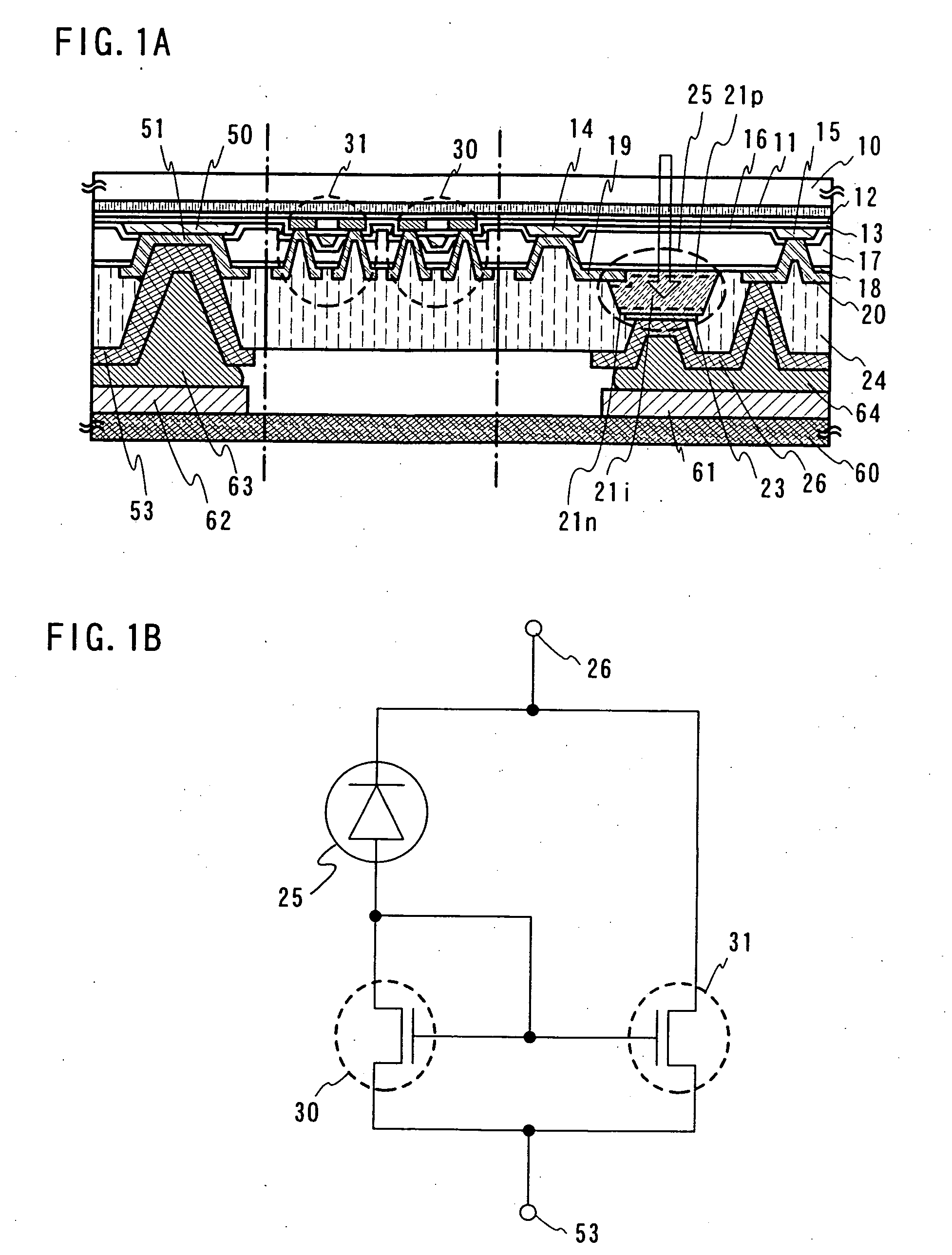
[0141] This embodiment shows a manufacturing process with reference to FIGS. 8A and 8B in which the second electrode pattern is different from that shown in the embodiment mode. The same reference numeral as that in FIGS. 1A to 3C is given to the same part in FIGS. 8A and 8B except for the second electrode pattern. Although FIGS. 8A and 8B don't show the amplifier circuit, it is formed as well as in the embodiment mode.

[0142] Initially, the processes up to forming the photoelectric conversion layer and forming the metal film to become the second electrode afterward are performed according to the embodiment mode.

[0143] In order to decrease the number of masks and processes, in this embodiment, after forming a second electrode 823 made of Ti, etching gas is changed, and then a photoelectric conversion layer including an amorphous silicon film is etched in a self-aligning manner using the resist mask 822 used for forming the second electrode 723. FIG. 8A shows the cross-sectional vie...

embodiment 3

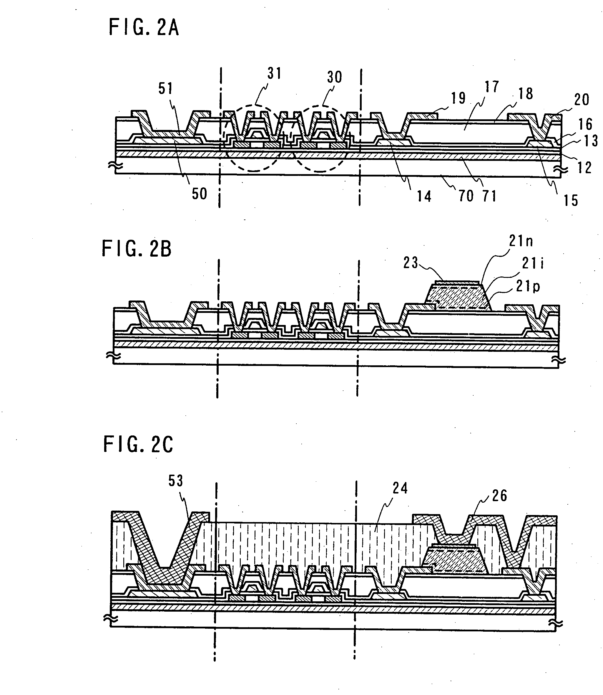
[0150] In contrast with the above embodiment showing the example of the amplifier circuit using only the n-channel TFT, this embodiment shows an example of an operational amplifier using a plurality of n-channel TFTs and p-channel TFTs.

[0151] Initially, a first photo mask is used to form a resist mask and etching is performed so that an island-shaped semiconductor layer is formed as well as in the embodiment mode. In this step, the island-shaped semiconductor layer is formed on the tungsten film and the base insulating film 912 over the glass substrate.

[0152] Next, a small amount of impurity element (boron or phosphorus) is doped if necessary in order to control the threshold of the TFT. Here, the ion-doping method is performed in such a way that diborane (B2H6) is excited to be plasma and it is added to the island-shaped semiconductor layer without mass-separation.

[0153] Next, the surface of the silicon film is washed at the same time as removing the oxide film by the etchant in...


PUM


Abstract

The object of the present invention is to miniaturize the area occupied by the element and to integrate a plenty of elements in a limited area so that the sensor element can have higher output and smaller size. In the present invention, higher output and miniaturization are achieved by uniting a sensor element using an amorphous semiconductor film (typically an amorphous silicon film) and an output amplifier circuit including a TFT with a semiconductor film having a crystal structure (typically a poly-crystalline silicon film) used as an active layer over a plastic film substrate that can resist the temperature in the process for mounting such as a solder reflow process. According to the present invention, the sensor element that can resist the bending stress can be obtained.

Description

BACKGROUND OF THE INVENTION [0001] 1. Field of the Invention [0002] The present invention relates to a semiconductor device having a sensor element and a circuit including a thin film transistor (hereinafter referred to as a TFT) and to its manufacturing method. [0003] It is noted that the semiconductor device herein indicates a general device that can function by utilizing semiconductor characteristic. An electro-optical device, a semiconductor circuit, and an electronic apparatus are included in the semiconductor device. [0004] 2. Related Art [0005] Conventionally, there are a sensor element using a single-crystal silicon substrate and a sensor element using an amorphous silicon film as a solid imaging element. [0006] The characteristic of the sensor element using the single-crystal silicon substrate is that high output can be obtained by manufacturing an output amplifier circuit on the single-crystal silicon substrate and by integrating this output amplifier circuit with the sens...

Claims


Application Information

Patent Timeline
IPC IPC(8): H01J40/14H01L21/82H01L27/146H01L27/14H01L31/00H01L31/10
CPCH01L27/1214H01L27/14665H01L27/14609H01L27/1266H01L2224/16225H01L27/1218H01L27/146H01L31/10
Inventor MARUYAMA, JUNYATAKAYAMA, TORUMORISUE, MASAFUMIWATANABE, RYOSUKESUGIYAMA, EIJIOKAZAKI, SUSUMUNISHI, KAZUOKOYAMA, JUNOSADA, TAKESHIMATSUZAKI, TAKANORI
Owner SEMICON ENERGY LAB CO LTD
Why Eureka
Try Eureka