[0048]FIG. 3 is a graphical image of an Asymmetric
MOSFET transistor structure 300 with local resistor ballasting according to the present invention. It is Asymmetric in that the drain 304 resistance is not equal to the source 302 resistance. An
advantage of the present invention is that adding a local resistor element Asymmetrically introduces resistor ballasting effects in the drain structure 304 without requiring corresponding resistor structures on the source side 302 or either OP block 310. Through resistor ballasting, the RF ESD benefits of a high-resistance structure under prior art techniques can be accomplished with a medium or
low resistance structure. A one to 100
Ohm local resistor structure can thus accomplish the ESD benefits equivalent to a
mega-
Ohm large resistor incorporated into the structure through prior art techniques. Using a small resistor on the order of the
contact hole size reduces capacitive and inductive effects. Other solutions such as diffused resistors or even wire interconnects are area intensive and lead to poor Q values due to inductive and capacitive effects. Using the local resistor 320, good ESD ballasting is achieved without RF degradation effects.
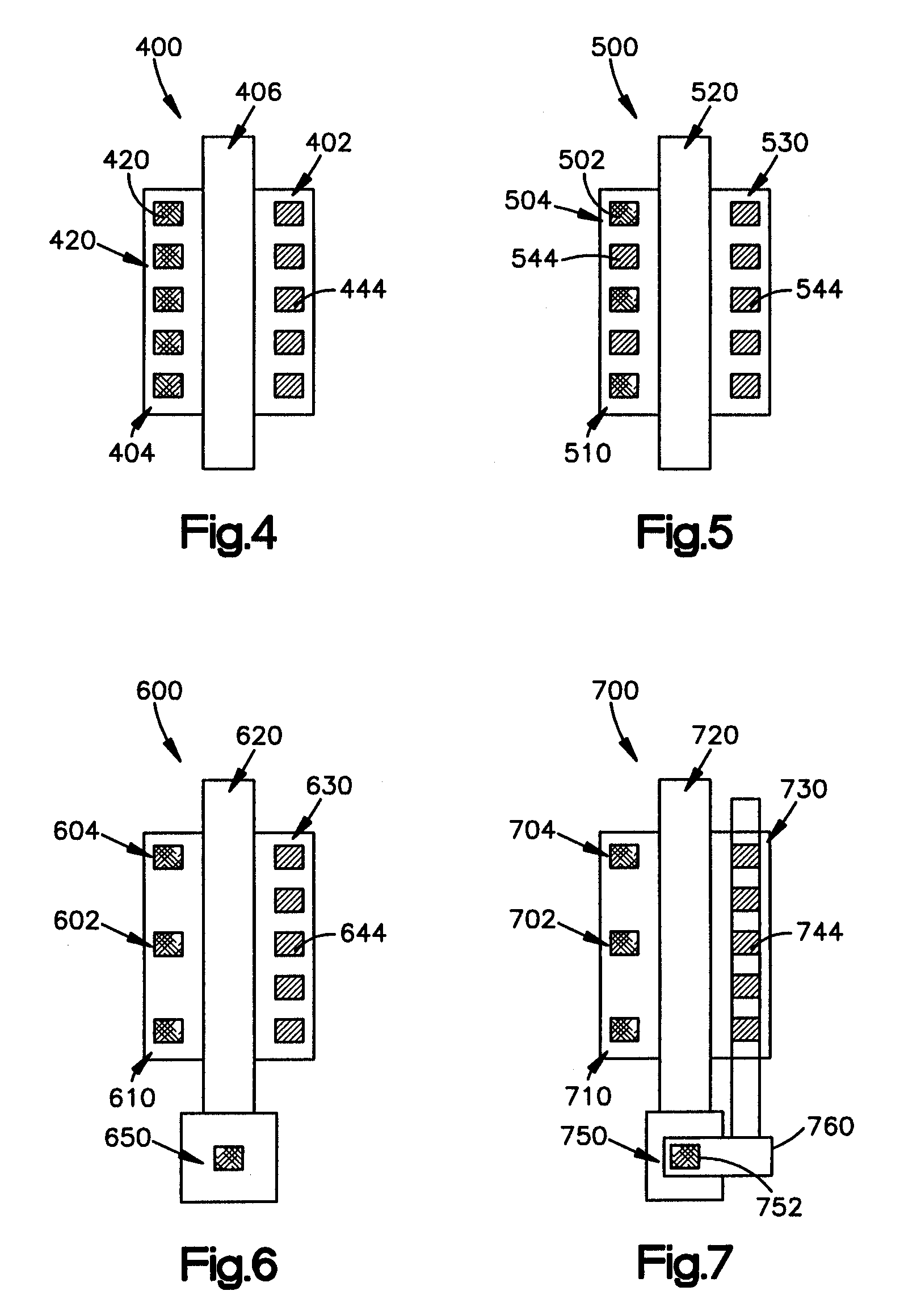
[0049]FIG. 4 is a graphical image of another Asymmetric
MOSFET transistor structure 400 according to the present invention with local resistor 422 ballasting interdigited into the contact structures 420. Adding a local resistor element 422 introduces ballasting in the drain structure 404. Here the local resistor ballasting provides satisfactory ESD and latchup protection, obviating the need for
salicide block
mask structures. Using a small resistor 422 on the order of the
contact hole size reduces capacitive and inductive effects. Other solutions such as diffused resistors or even wire interconnects are area intensive and lead to poor Q values due to inductive and capacitive effects. Using the local resistor 422, an
advantage is that good ESD ballasting is achieved without RF degradation effects. Additionally, by choosing the location of the contact 444 relative to the resistor 422, non-uniform thermal distribution can be compensated and improved lateral
current distribution is achieved.
[0050]FIG. 5 is a graphical image of a
Silicon-on-insulator (SOI) Asymmetric
MOSFET transistor structure 500 according to the present invention with local resistor ballasting interdigited into the contact structures 502 and 504
and gate resistor structure 520. Adding a local resistor element 504 introduces ballasting in the drain structure 510. Using a small resistor 504 on the order of the contact
hole size reduces capacitive and inductive effects. Other solutions such as diffused resistors or even wire interconnects are area intensive and lead to poor Q values due to inductive and capacitive effects. Using the local resistor 504, good ESD ballasting is achieved without RF degradation effects. In SOI technology, failure mechanisms unique to SOI occur between the gate 520 and the drain 510, and the gate 520 and the source 530. Hence, in SOI having a
high resistance element in series with the gate can eliminate Charge Device Model failure mechanisms observed in advanced SOI microprocessors.
[0051] An important
advantage of the present invention illustrated in FIG. 5 is that the local resistor may be selectively introduced into a specified number of contact regions responsive to the current flow modification desired. As illustrated, three local resistors 504 are introduced into three specified contact regions 502 in the drain region 510, into an alternating arrangement with drain contacts 504. Thus, the present invention enables the introduction of non-uniform resistance on one side only of the source-drain structure. This enables spreading out current flow, or optimizing current flow, on the drain side by the selective placement of the local resistors 504. This is very important in
high current flow applications, because current flow through a transistor source-drain structure is not uniform. The present invention enables modulation of that current flow through the selective placement of the local resistors 504.
[0052] The ballasting local resistors discussed thus far are formed within contact holes within transistor drain structures. Where the structural dimensions available to the local resistors are limited to the size of contact holes under the present invention, their resistance values are also necessarily limited by this physical constraint. Generally, the drain contact hole local resistors resistance values cannot provide
mega-Ohm values, which some applications may demand.
[0053]FIG. 6 is a graphical image of an Asymmetric MOSFET transistor structure 600 according to the present invention with local resistor ballasting in the drain
and gate structures. As discussed above, adding a contact local resistor element 604 introduces ballasting in the drain structure 610. Using a small resistor on the order of the contact
hole size 602 reduces capacitive and inductive effects. Other solutions such as diffused resistors or even wire interconnects are area intensive and lead to poor Q values due to inductive and capacitive effects. Using one or more drain contact local resistors 604 provides good ESD ballasting without RF degradation effects. Another advantage of the present invention is the addition of a local resistor 650 to the gate 620. This local resistor 650 cuts back the current flow through the gate structure 620, which improves the current leakage characteristics of the gate 620. Placing the local resistance 650 in series with the gate 620 also improves the impedance of the gate structure 620 and thereby improves ESD protection for the MOSFET 600.

