Multi-layer optical information storage medium and method of making the same
a technology of optical information storage media and multi-layer material, which is applied in the direction of data recording, record carrier material, instruments, etc., can solve the problems of reducing process yield, reducing process yield, and relatively brittle pmma material
- Summary
- Abstract
- Description
- Claims
- Application Information
AI Technical Summary
Benefits of technology
Problems solved by technology
Method used
Image
Examples
example 1
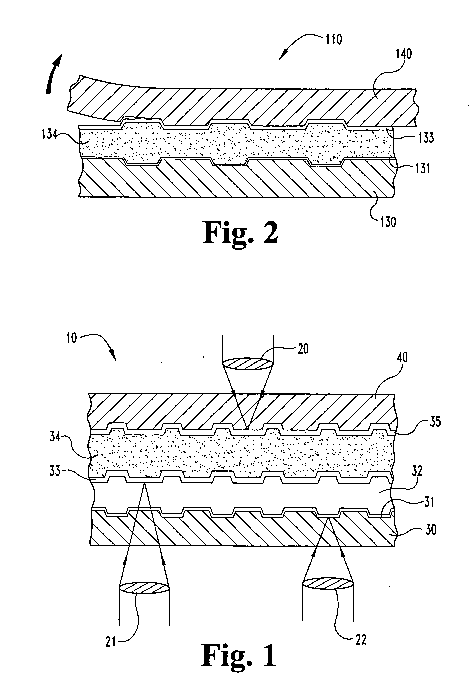
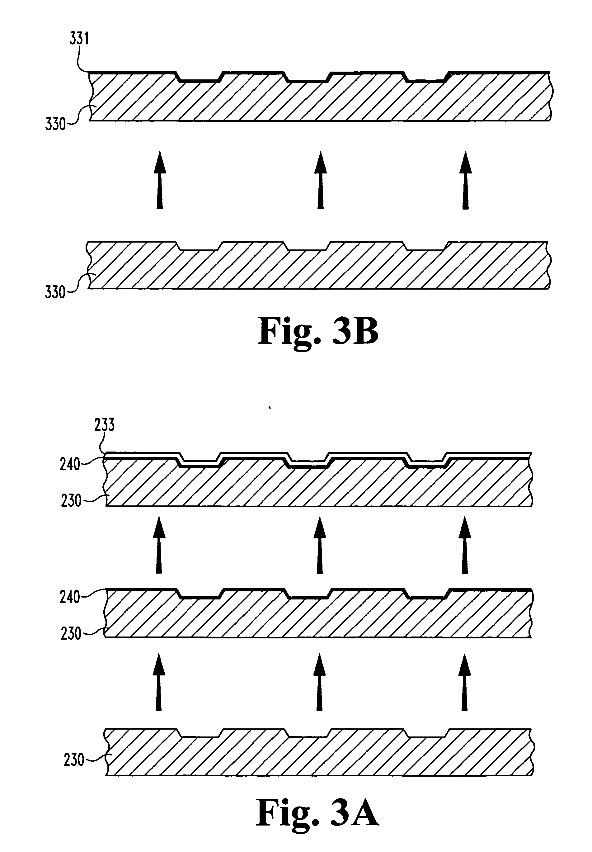
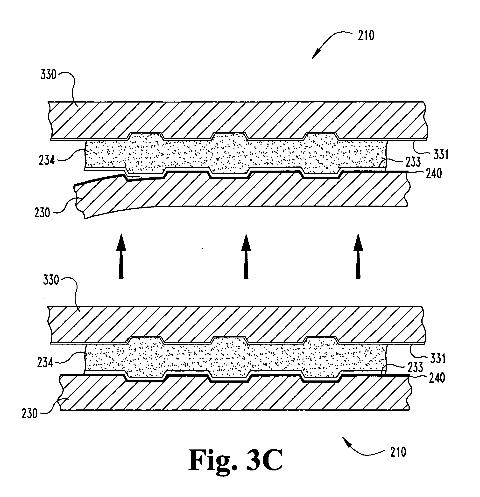
[0043] Referring now to FIG. 6, one embodiment is a manufacturing process suitable for making optical storage media that includes multiple information layers such as, for example, a DVD-14. Two 0.6 mm thick polycarbonate substrates are formed by injection molding using and stampers to form separate substrates 230 and 330. Substrates 230, 330 each have separate information features. Substrate 230 is subsequently sputter coated to form a “parting layer”240 that is 5 nm thick. The target used to form the parting layer on 240 is made with tin that has a minimum purity of 99.99% by weight. Afterwards, substrate 230 is sputter coated to form a 35 nm thick semi-reflective layer. The sputtering target used to form the semi-reflective layer on 230 is a silver alloy comprising: 1.1% by weight copper and 98.9% by weight of silver. Substrate 330 is coated with a 10 nm thick semi-reflective layer. The composition of the sputtering target used to form the semi-reflective layer on substrate 330 is...
example 2
[0045] The embodiment illustrated in this example is similar to the embodiment illustrated in Example 1, except that the parting layer is made from a sputtering target of antimony with a purity of about 99.99% weight minimum applied by a sputtering process.
example 3
[0046] Example 3 is similar to Example 2, except that the parting material is applied by sputtering using a sputtering target comprising lead with a minimum purity of about 99.99% by weight. Substrate 210 with two information layers 233 and 331, and another 0.6 mm polycarbonate substrate with only one information layer having a reflective layer made of an aluminum alloy of 45 nm thick are joined together. As illustrated in FIG. 5 the finished disc comprises three information layers.
PUM
| Property | Measurement | Unit |
|---|---|---|
| diameter | aaaaa | aaaaa |
| diameter | aaaaa | aaaaa |
| diameter | aaaaa | aaaaa |
Abstract
Description
Claims
Application Information


