Conductive paste, method for producing same, circuit board using such conductive paste and method for producing same

a technology of conductive paste and conductive paste, which is applied in the field of conductive paste, can solve the problems of difficult to solve, difficult to achieve mixing ratio, and severe request for manufacturing cost, and achieve the effects of reducing viscosity, improving contact state, and high dispersibility

Inactive Publication Date: 2005-08-11
PANASONIC CORP
View PDF13 Cites 31 Cited by
  • Summary
  • Abstract
  • Description
  • Claims
  • Application Information

AI Technical Summary

Benefits of technology

[0037] Thus, conductive particles in conductive paste are dispersed with high dispersibility into a binder based on thermosetting resin in order to manufacture conductive paste with lowered viscosity, and it is possible to improve the state of contact between the conductive particles in inner via-hole and to avoid variation of the state of contact. Accordingly, it is possible to provide a conductive paste capable of meeting both purposes of improving the connection reliability and reducing the cost by improving the productivity, and to realize a highly reliable circuit forming board using the conductive paste.

Problems solved by technology

Also, in the case of electronic equipment such as household portable telephones, there has been a severe request for the manufacturing cost.
However, the conductive paste involves the following three problems, and it is difficult to solve these problems and to achieve both purposes of improving the conducting connection reliability and reducing the cost by improving the productivity.
However, in mixing of solid conductive particles and liquid binder, the mixing ratio possible for making a paste is limited, and if the viscosity is too high, it will affect the smoothness of filling into via.
Since metallic foil 16 and insulating board 12 are heated and pressurized to form inner via-holes, if a lot of volatile component is contained in conductive paste 14, the steam pressure in the inner via-hole will be increased during heating and there is a possibility that defective connection takes place due to swelling.

Method used


Image

  • Conductive paste, method for producing same, circuit board using such conductive paste and method for producing same
  • Conductive paste, method for producing same, circuit board using such conductive paste and method for producing same
  • Conductive paste, method for producing same, circuit board using such conductive paste and method for producing same

Examples


embodiment 1

Preferred Embodiment 1

[0040] The preferred embodiment 1 will be described with reference to the drawings.

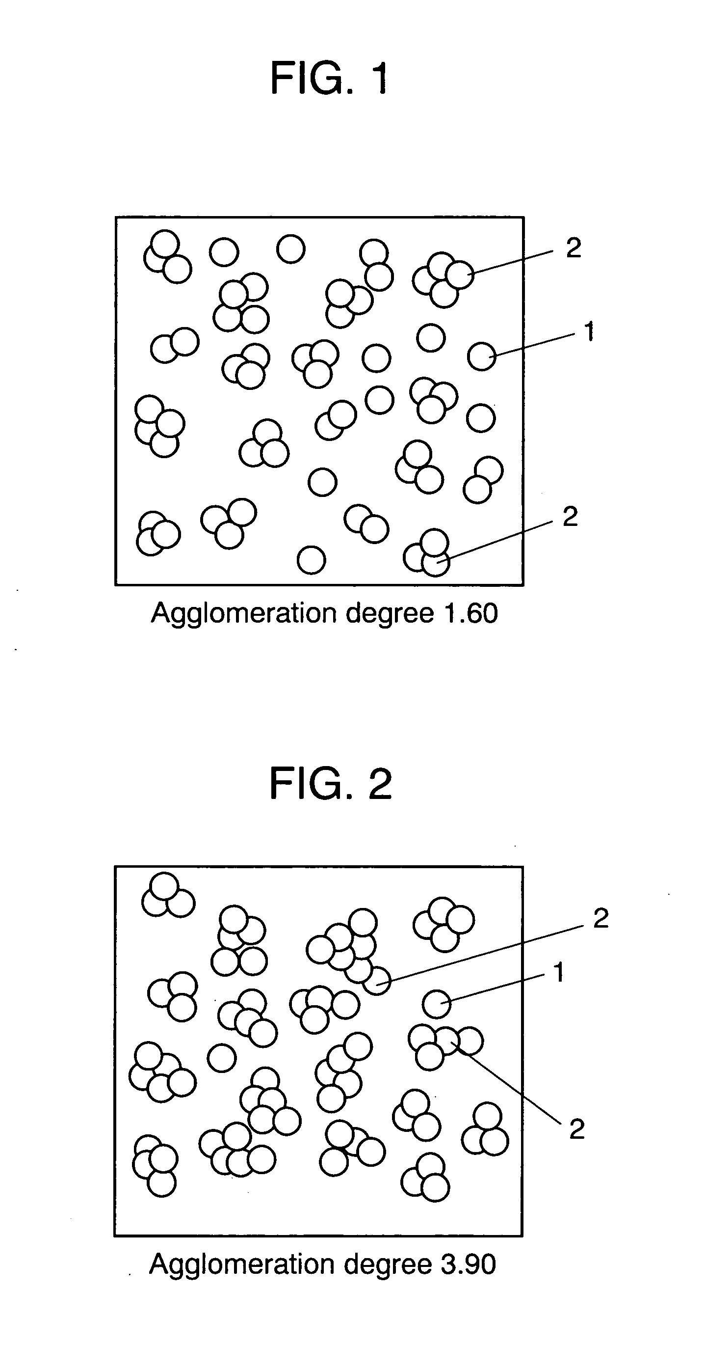
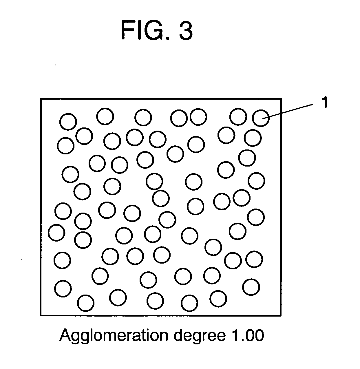
[0041] To describe the features of the present invention briefly, it is to accurately control the agglomeration and particle size distribution with respect to metallic powder such as copper, silver or gold, alloy powder or metal powder coated with different kinds of metal as conductive particles of conductive paste. As a measuring instrument for particle size distribution of conductive particles, a laser diffraction scattering system is widely employed in the power industry, and instruments such as Microtrack of Nikkiso Co., Ltd make as wet type, and HELOS of SYMPATECH make as dry type are well-known.

[0042]FIG. 1 is a plan view schematically showing a state of agglomeration of copper powder of conductive paste related to the preferred embodiment 1. As shown in FIG. 1, the copper particle as conductive particle related to the preferred embodiment 1 is an aggregate of primary par...

embodiment 2

Preferred Embodiment 2

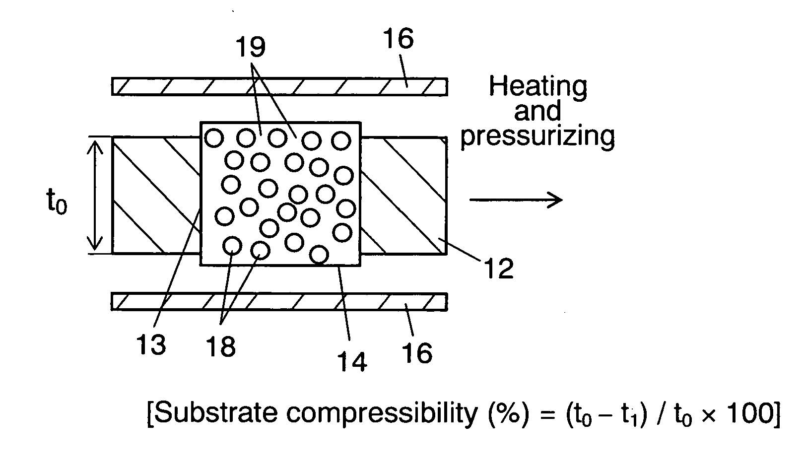
[0073] The circuit forming board related to the preferred embodiment 2 of the present invention will be described in the following.

[0074]FIG. 6A to FIG. 6G are sectional views showing the manufacturing process of a circuit forming board related to the present invention.

[0075] First, as shown in FIG. 6A, non-woven cloth of aramid fiber is impregnated with epoxy resin, and PET (polyethylene phthalate) film 11 of 20 μm thick which is formed by applying a releasing agent of silicone type or the like is laminated by a laminator onto both surfaces of insulating board (prepreg sheet) 12 in a state of being half-hardened (B-stage) which is 120 μm in thickness and 500 mm×340 mm in size.

[0076] Subsequently, as shown in FIG. 6B, through-hole 13 of φ200 m in via-diameter is formed by a carbon dioxide laser beam at a predetermined position of insulating board (prepreg sheet) 12.

[0077] Next, as shown in FIG. 6C, conductive paste 4 manufactured in the preferred embodiment...

embodiment 3

Preferred Embodiment 3

[0100] A circuit forming board using conductive paste with particle size distribution controlled and its conductive paste will be described in the following.

[0101] The configuration other than conductive particles in the conductive paste related to the preferred embodiment 3 and the manufacturing method for a circuit forming board using the conductive paste are same as described in the preferred embodiment 1 and preferred embodiment 2, and the detailed description is omitted.

[0102]FIG. 4A and FIG. 4B are diagrams showing one embodiment of particle size distribution of copper powder related to the preferred embodiment 3, each of which represent same sample.

[0103] Copper powder used in the preferred embodiment 3 is nearly the same as described in the preferred embodiments 1 and 2 in its manufacturing method. As a method of improving the dispersibility of conductive paste, it is given at least two peaks of different particle diameters.

[0104] Specifically, as c...


PUM

PropertyMeasurementUnit
specific surface areaaaaaaaaaaa
particle diameteraaaaaaaaaa
particle size distributionsaaaaaaaaaa

Abstract

It is intended to reliably form high-quality via-hole conductor with less variation, and to realize a circuit forming board having excellent connection reliability. It provides a conductive paste comprising primary particles and agglomerate of primary particles, conductive particles of 0.5 to 20 μm in average particle diameter and 0.07 to 1.7 m2/g in specific surface area, and a binder based on thermosetting resin, and also provides an inexpensive circuit forming board with high connection reliability by using the paste.

Description

TECHNICAL FIELD [0001] The present invention relates to a conductive paste which can be used for filling via-holes for electrical connection between compositions of conductive paste used for a circuit forming board used in various electronic apparatuses, particularly between layers in a multi-layered board, a method of manufacturing the conductive paste, a circuit forming board using the conductive paste, and its manufacturing method. BACKGROUND ART [0002] Recently, as electronic apparatuses are rapidly reduced in size and increased in density, double-sided and multi-layered boards are more and more employed in place of conventional single-sided boards as circuit forming boards for mounting electronic components, and developments are now directed toward providing high-density circuit forming boards capable of integrating as many circuits as possible thereon. [0003] In a circuit forming board, instead of layer-to-layer connection by through-hole machining and plating as is convention...

Claims


Application Information

Patent Timeline
Patent Type & Authority Applications(United States)
IPC IPC(8): H01B1/20H01B1/22H05K1/09H05K3/40
CPCH01B1/22H05K1/095H05K3/4069Y10T29/49126H05K2201/0355H05K2203/1461Y10T428/2982H05K2201/0266
Inventor SUGITA, YUICHIROTAKENAKA, TOSHIAKI
Owner PANASONIC CORP
Why Eureka
Try Eureka