Method and apparatus for high-speed thickness mapping of patterned thin films

a technology of patterned thin films and thickness mapping, applied in photomechanical equipment, instruments, optics, etc., can solve the problems of reducing the efficiency of measurement spot density, and requiring substantial space in the semiconductor fabrication cleanroom. , to achieve the effect of optimizing the density of measurement spots, improving image quality, and reducing the distance between spatial locations

Inactive Publication Date: 2005-08-11
FILMETRICS
View PDF1 Cites 40 Cited by
  • Summary
  • Abstract
  • Description
  • Claims
  • Application Information

AI Technical Summary

Benefits of technology

[0019] In another embodiment, the invention provides an apparatus and method for improving image quality by slant scanning. Slant scanning reduces the distance between spatial locations imaged on a portion of a patterned wafer by relatively translating the wafer at a non-normal angle with respect to the line being imaged by the one-dimensional spectrometer. A means for translating the wafer in this fashion is provided as a subsystem integral to the wafer imaging system. Generally, measurement spot density increases as the wafer pattern angle increases from a normal angle (i.e. zero degrees with respect to the scanning direction) to an angle of about + / −90 degrees, with an optimal angle occurring somewhere within that range. Thus, the invention allows a patterned wafer to be imaged by scanning at a desired non-normal angle, or slant, with respect to the line being imaged to optimize measurement spot density according to the particular configuration of the imaging system.

Problems solved by technology

Because the areas covered by these features are generally unsuitable for measurement of film properties, specific measurement sites called “pads” are provided at various locations on the wafer.
This small pad size presents a challenge for the film measurement equipment, both in measurement spot size and in locating the measurement pads on the large patterned wafer.
This is because current systems that measure thickness on patterned wafers are slow, complex, expensive, and require substantial space in the semiconductor fabrication cleanroom.
Such systems are too slow to be used concurrently with semiconductor processing, so the rate of semiconductor processing must be slowed down to permit film monitoring.
The result is a reduced throughput of semiconductor processing and hence higher cost.
Because the resolution and speed of available CCD imagers are limited, higher magnification sub-images of the wafer are required to resolve the measurement pads.
These additional sub-images require more time to acquire and also require complex moving lens systems and mechanical translation equipment.
The result is a questionable advantage in speed and performance over traditional microscope / pattern recognition-based spectral reflectance systems.

Method used


Image

  • Method and apparatus for high-speed thickness mapping of patterned thin films
  • Method and apparatus for high-speed thickness mapping of patterned thin films
  • Method and apparatus for high-speed thickness mapping of patterned thin films

Examples


first embodiment

A System for Measurements at an Angle

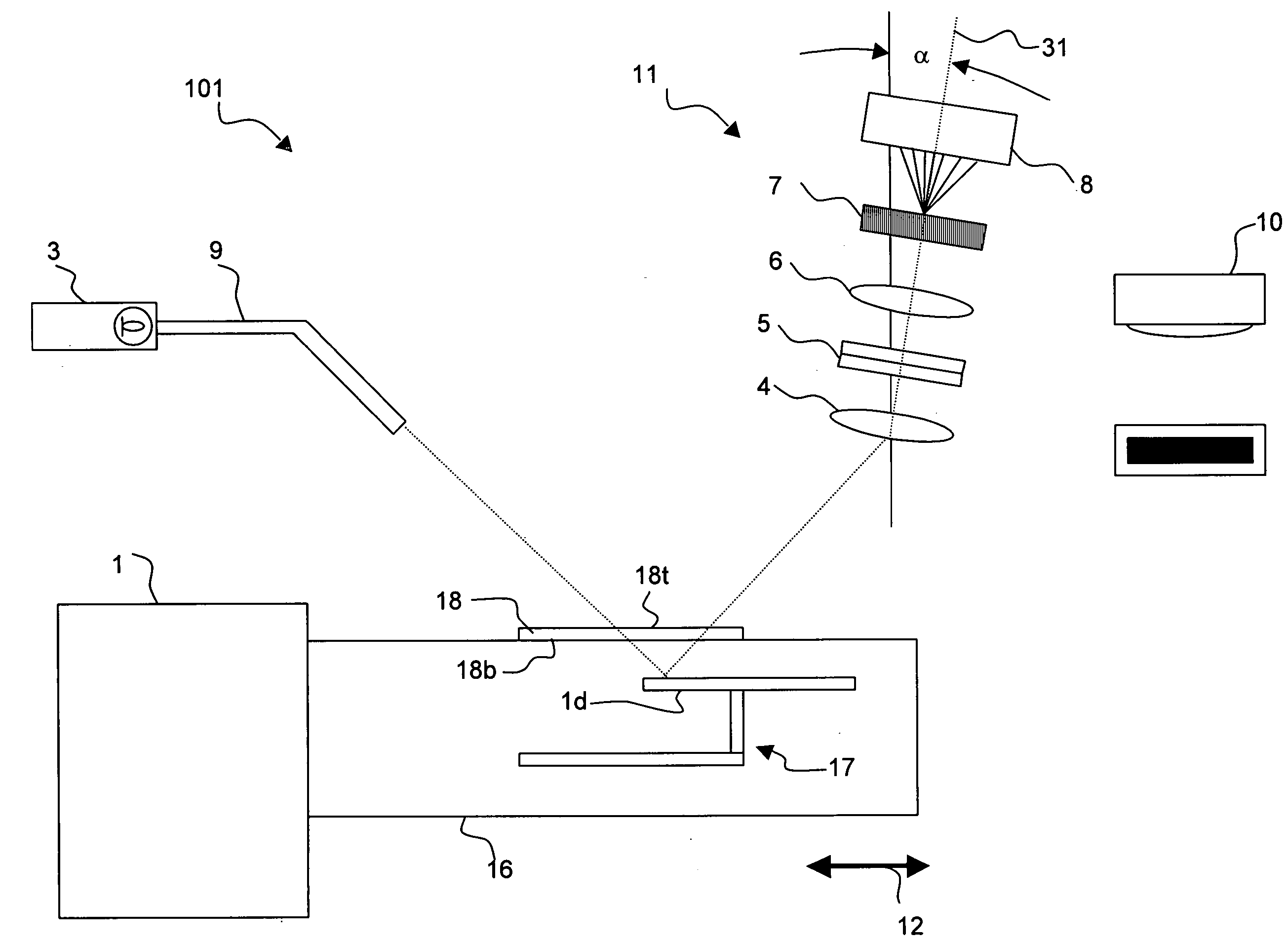
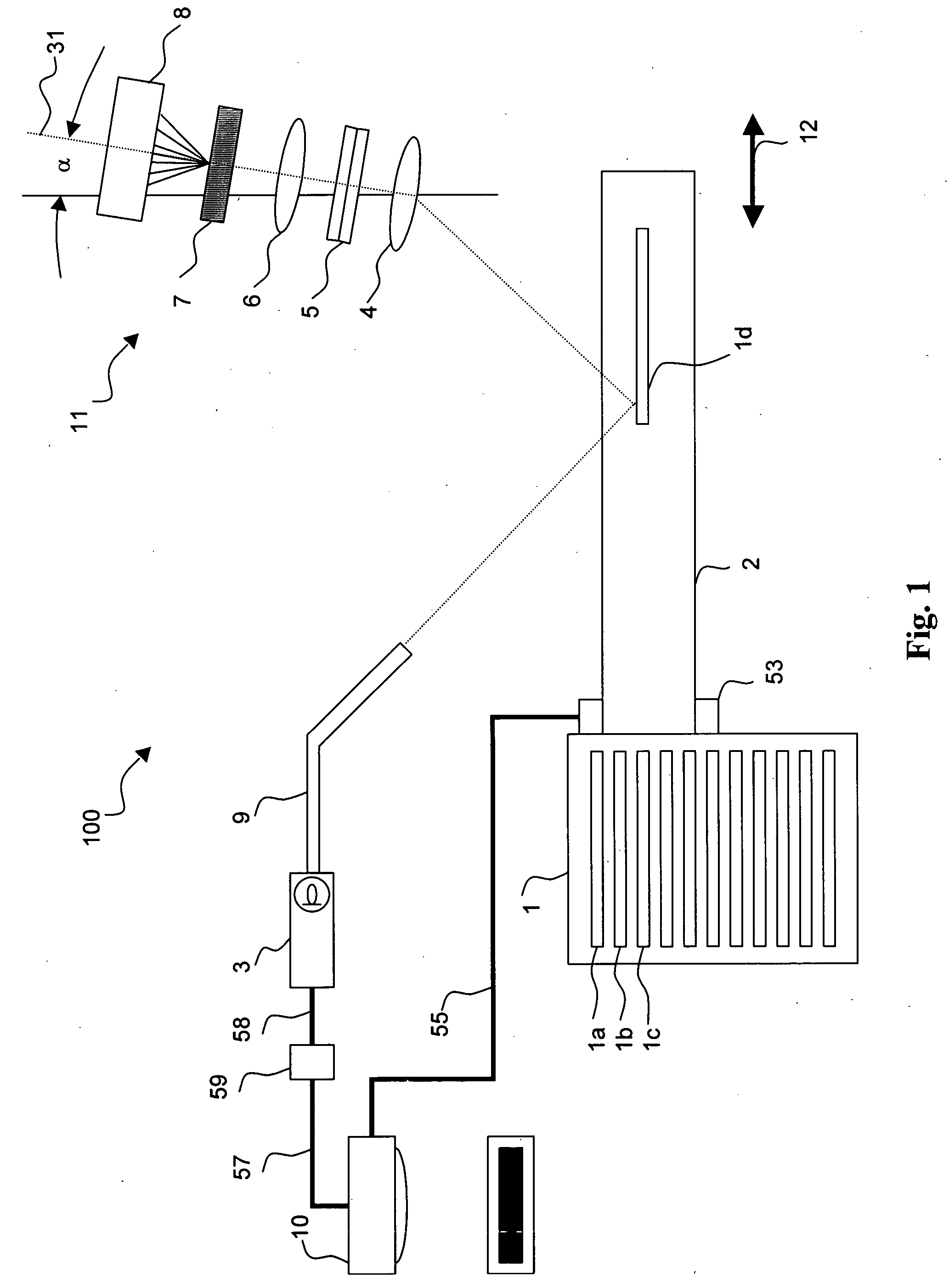
[0069] A first embodiment of an imaging system 100 in accordance with the subject invention, suitable for use in applications such as measuring the thickness of transparent or semi-transparent films, is illustrated in FIG. 1. Advantageously, the film to be measured ranges in thickness from 0.001 μm to 50 μm, but it should be appreciated that this range is provided by way of example only, and not by way of limitation. This embodiment is advantageously configured for use with a wafer transfer station 1 to facilitate rapid measurement of a cassette of wafers. The station houses a plurality of individual wafers 1a, 1b, 1c, and is configured to place a selected one of these wafers, identified with numeral 1d in the figure, onto a platform 2. Each of wafers 1a, 1b, 1c, and 1d has a center point and an edge. This embodiment also comprises a light source 3 coupled to an optical fiber 9 or fiber bundle for delivering light from the light source 3 to the ...

commercial embodiment

[0095] A commercial embodiment of a system according to the invention will now be described. The manufacturers of the components of this system are as identified in the previous example, with the exception of the lens assembly used in the spectrometer. In lieu of standard lenses designed for use with 35 mm cameras, this embodiment employs high quality lenses and mirrors manufactured by Optics 1 of Thousand Oaks, Calif. These lenses and mirrors are such that the modulation transfer function (MTF) for a plurality of alternating black and white line pairs having a density of about 40 line pairs / mm is greater than 70% over the entire wavelength range of interest.

[0096] This system is configured to measure the thicknesses of individual layers of a sample, e.g., a patterned semiconductor wafer, at desired measurement locations. The coordinates of these desired measurement locations are provided to the system. Rather than rely on complicated and unreliable traditional pattern recognition ...

embodiment

Method of Operation—Commercial Embodiment

[0121]FIG. 11 is a flowchart of the method of operation followed by the current commercial embodiment for each layer in the sample being evaluated. The sample may be a semiconductor wafer or some other sample. In step 1100, the reflectance spectra for a plurality of spatial locations on the surface of a sample are simultaneously captured. The spatial locations may be in the form of a line, or some other shape, such as a curved shape, although in the current commercial embodiment, the locations are in the form of a line.

[0122] In step 1004, an evaluation is made whether all or a substantial portion of the entire surface has been scanned. If not, step 1102 is performed. In step 1102, a relative translation is performed between the surface of the sample and the light source and sensor used to perform the capture process. Again, this step can occur by moving the surface relative to one or the other of the light source and sensor, or vice-versa. ...


PUM

PropertyMeasurementUnit
angleaaaaaaaaaa
thickaaaaaaaaaa
thicknessaaaaaaaaaa

Abstract

An apparatus or method captures reflectance spectrum for each of a plurality of spatial locations on the surface of a patterned wafer. A spectrometer system having a wavelength-dispersive element receives light reflected from the locations and separates the light into its constituent wavelength components. A one-dimensional imager scans the reflected light during translation of the wafer with respect to the spectrometer to obtain a set of successive, spatially contiguous, one-spatial dimension spectral images. A processor aggregates the images to form a two-spatial dimension spectral image. One or more properties of the wafer, such as film thickness, are determined from the spectral image. The apparatus or method may provide for relatively translating the wafer at a desired angle with respect to the line being imaged by the spectrometer to enhance measurement spot density, and may provide for automatic focusing of the wafer image by displacement sensor feedback control. The spectrometer system may include an Offner optical system configured to twice pass light reflected from the wafer and received by the imager.

Description

[0001] This application claims benefit of U.S. Provisional Application 60 / 584,982 filed Jul. 2, 2004, which is hereby fully incorporated by reference herein. [0002] This application is a continuation-in-part of U.S. patent application Ser. No. 09 / 899,383, filed Jul. 3, 2001, which is a continuation-in-part of U.S. patent application Ser. No. 09 / 611,219, filed Jul. 6, 2000, both of which are hereby fully incorporated by reference herein. This application is related to U.S. patent application Ser. No. ______, Howrey Dkt. No. 02578.0006.CPUS02, filed Feb. 10, 2005, which is hereby fully incorporated by reference herein.BACKGROUND OF THE INVENTION [0003] This invention relates generally to the field of film thickness measurement, and more specifically, to the field of film measurement in an environment, such as semiconductor wafer fabrication and processing, on which a layer with an unknown thickness resides on a patterned sample. [0004] Many industrial processes require precise control...

Claims


Application Information

Patent Timeline
Patent Type & Authority Applications(United States)
IPC IPC(8): G01B11/06G01N21/55G01N21/84G01N21/95G03F7/20
CPCG01B11/0625G01N21/55G03F7/70483G01N21/956G01N21/8422
Inventor CHALMERS, SCOTT A.GEELS, RANDALL S.
Owner FILMETRICS
Why Eureka
Try Eureka