cMUT devices and fabrication methods

a technology of capacitive micromachined ultrasonic transducers and fabrication methods, which is applied in the direction of mechanical vibration separation, instruments, pulse techniques, etc., can solve the problems of complex fabrication process, inability to assemble a cmut device into a cmut device, and inability to integrate post-process complimentary metal oxide semiconductors (“cmos”), so as to reduce device parasitic capacitance and improve electrical performance.

Inactive Publication Date: 2005-08-11
GEORGIA TECH RES CORP
View PDF60 Cites 242 Cited by
  • Summary
  • Abstract
  • Description
  • Claims
  • Application Information

AI Technical Summary

Benefits of technology

[0014] The present invention comprises cMUT array transducer fabrication methods and systems. The present invention provides cMUTs for imaging applications that can be fabricated directly on top of CMOS electronics, which can be especially useful in medical imaging applications. The cMUTs can be fabricated on dielectric or transparent subst

Problems solved by technology

The high process temperatures (approximately 900 degrees Celsius) of LPCVD make post-process complimentary metal oxide semiconductor (“CMOS”) integration impossible.
Yet, such approaches do not allow a CMOS device to be fabricated into a cMUT device, but rather merely bond a CMOS device to a cMUT after fabrication.
A major drawback to this approach is the complicated fabrication process.
This technique, however, both generates a large cMUT cavity, approximately 4000 Angstroms or larger, and requires high DC bias voltages.
Additionally, the PECVD process temperature (approximately 400-500 degrees Celsius) is still too high for CMOS integration as it can destroy CMOS electronics.

Method used


Image

  • cMUT devices and fabrication methods
  • cMUT devices and fabrication methods
  • cMUT devices and fabrication methods

Examples


Embodiment Construction

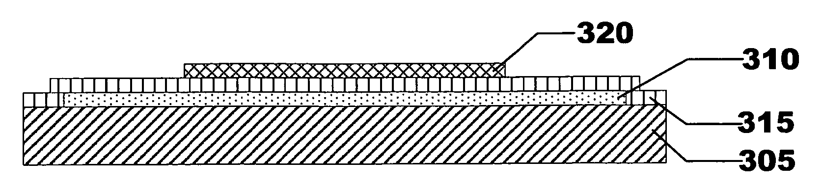
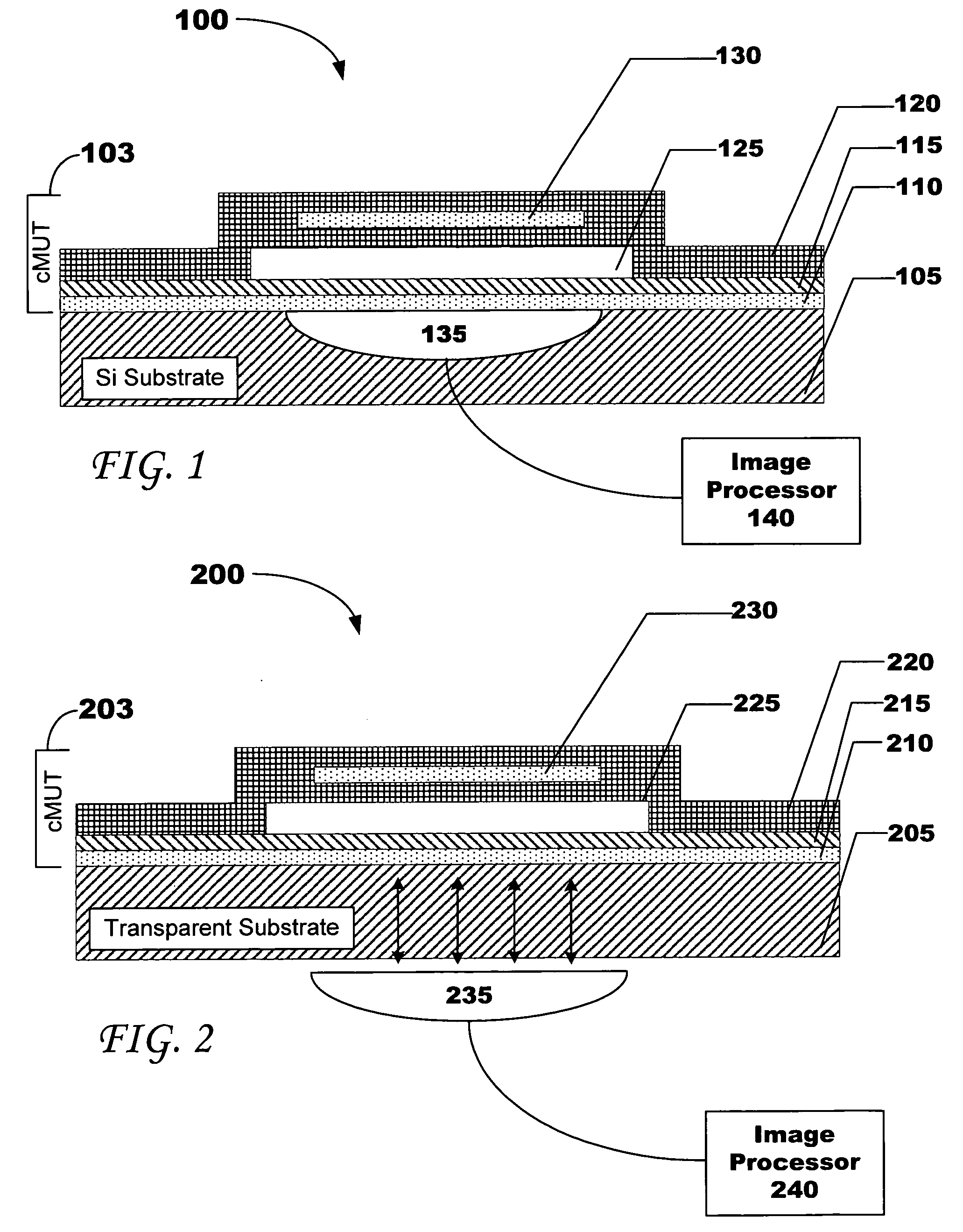
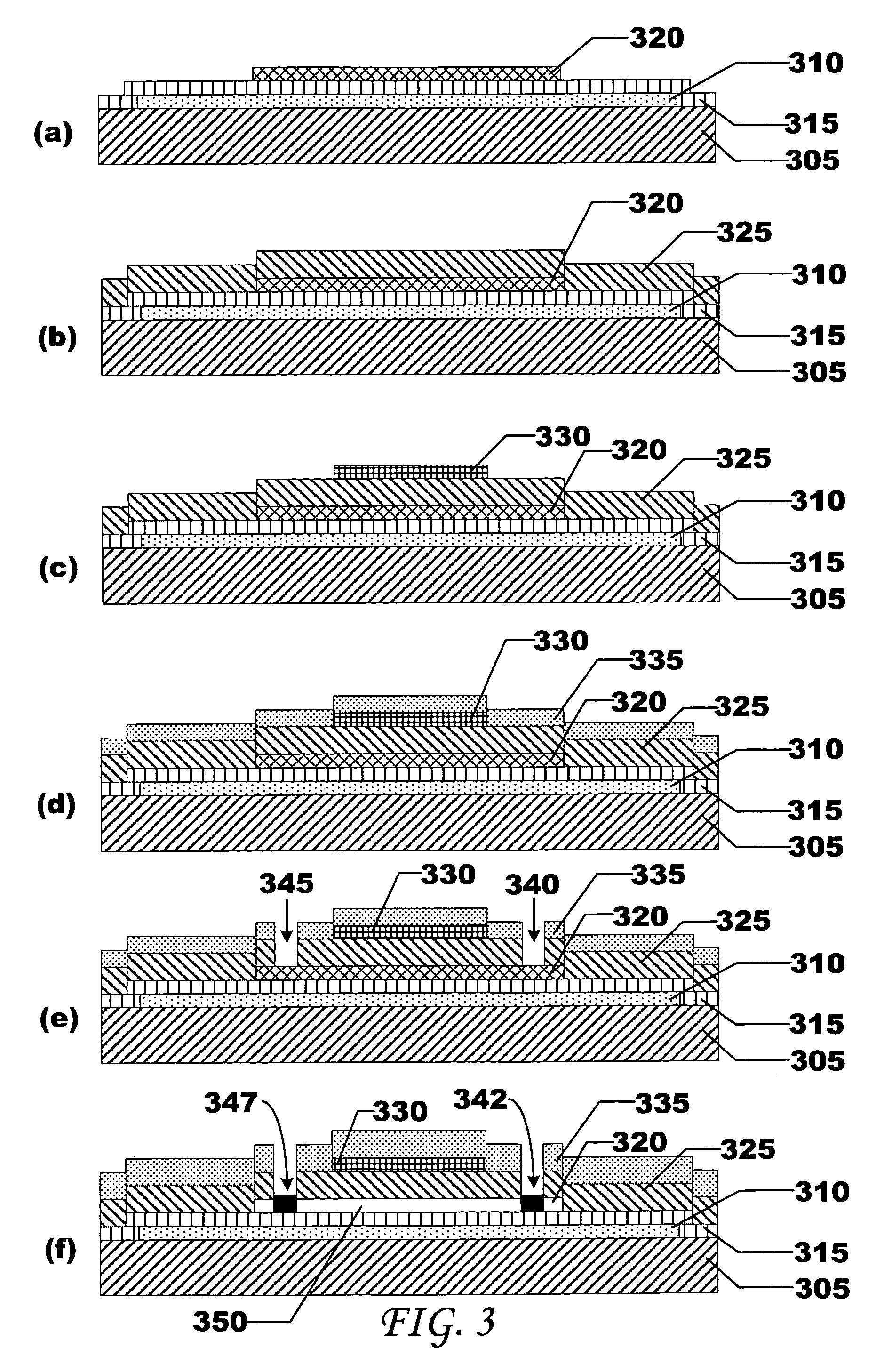
[0026] cMUTs have been developed as an alternative to piezoelectric ultrasonic transducers particularly for micro-scale and array applications. Since cMUTs are surface micromachined, they can be fabricated into one or two-dimensional arrays and customized for specific applications, and can have performance comparable to piezoelectric transducers in terms of bandwidth and dynamic range. A cMUT device typically incorporates a membrane, with an electrode, suspended above a conductive substrate or another electrode coupled to a substrate. The membrane can have elastic properties enabling it to fluctuate in response to stimuli. For example, stimuli may include, but are not limited to, external forces exerting pressure on the membrane and electrostatic forces applied through cMUT electrodes. cMUTs can transmit and receive acoustical waves. To transmit an acoustic wave, an AC signal and a large DC bias voltage are applied to the membrane. The DC voltage pulls down the membrane where the tr...


PUM


Abstract

Fabrication methods for capacitive-micromachined ultrasound transducers (“cMUT”) and cMUT imaging array systems are provided. cMUT devices fabricated from low process temperatures are also provided. In an exemplary embodiment, a process temperature can be less than approximately 300 degrees Celsius. A cMUT fabrication method generally comprises depositing and patterning materials on a substrate (400). The substrate (400) can be silicon, transparent, other materials. In an exemplary embodiment, multiple metal layers (405, 410, 415) can be deposited and patterned onto the substrate (400); several membrane layers (420, 435, 445) can be deposited over the multiple metal layers (405, 410, 415); and additional metal layers (425, 430) can be disposed within the several membrane layers (420, 435, 445). The second metal layer (410) is preferably resistant to etchants used to etch the third metal layer (415) when forming a cavity (447). Other embodiments are also claimed and described.

Description

CROSS REFERENCE TO RELATED APPLICATION AND PRIORTY CLAIM [0001] This Application claims the benefit of U.S. Provisional Application Ser. No. 60 / 542,378 filed on 6 Feb. 2004.TECHNICAL FIELD [0002] The invention relates generally to chip fabrication, and more particularly, to fabricating capacitive micromachined ultrasonic transducers and capacitive micromachined ultrasonic transducer imaging arrays. BACKGROUND [0003] Capacitive micromachined ultrasonic transducer (“cMUT”) devices generally combine mechanical and electronic components in very small packages. Typically, the mechanical and electronic components operate together. Because cMUTs are typically very small and have both mechanical and electrical parts, they are commonly referred to as micro-electronic mechanical systems (“MEMS”) devices. [0004] MEMS manufacturing processes have launched many innovations in many different technical fields. The medical device field has greatly benefited from MEMS technology. MEMS technology ena...

Claims


Application Information

Patent Timeline
IPC IPC(8): A61B8/02A61B8/12B06B1/02H01L21/00
CPCG01N29/2406B06B1/0292
Inventor DEGERTEKIN, F. LEVENTMCLEAN, JEFFREY JOHNKNIGHT, JOSHUA GLENN
Owner GEORGIA TECH RES CORP
Why Eureka
Try Eureka