Novel approach to improve line end shortening

a technology of line end and shortening, which is applied in the field of fabricating semiconductor structures, can solve the problems of insufficient narrow lb>1/b> to meet the requirements of a fast transistor, the inability to control the size of the photoresist less than about 100 nm, and the process latitude is improved, so as to achieve better control

Inactive Publication Date: 2005-09-01
TAIWAN SEMICON MFG CO LTD
View PDF9 Cites 13 Cited by
  • Summary
  • Abstract
  • Description
  • Claims
  • Application Information

AI Technical Summary

Benefits of technology

[0021] In a second embodiment, the method of the present invention is applied to the formation of an STI feature. A silicon nitride layer is formed on a substrate and then a hardmask such as silicon oxynitride is deposited on the nitride. Optionally, an organic or inorganic ARC is deposited on the hardmask to improve process latitude in a later photoresist patterning step. A photoresist layer is coated and patterned to form trench openings. First, an anisotropic etch is performed to transfer the pattern through the hardmask. Then the photoresist and hardmask are simultaneously etched isotropically to shrink the linewidth between trench openings with a plasma etch involving CXFY, H2, and optionally O2. The shrinkage in the active area between the trenches is better controlled than in conventional processes that require a photoresist trim prior to etch transfer through the hardmask. Likewise, the ends of the trenches are kept within specification by restricting lateral growth during the etch transfer. The photoresist is stripped and the pattern is etch transferred through the nitride and into the substrate to form shallow trenches which are then filled with a dielectric material such as SiO2.

Problems solved by technology

One shortcoming in state of the art lithography processes is that they are incapable of controllably printing features in photoresist smaller than about 100 nm.
Frequently, L1 is not narrow enough to meet the requirements for a fast transistor speed.
One problem associated with trimming photoresist 18 is that shortening occurs at line ends which can degrade device performance.
As a result, rough edges at the top of line 18b in FIG. 2b can easily generate grooves in the sidewalls of line 18 that are transferred through ARC 17a into hardmask 16a which is detrimental to device performance.
However, in most instances, this correction is not possible because there is not enough room in the mask design to compensate for LES.
Although LES is an important issue in fabricating integrated circuits, there is no prior art that mentions how to minimize the problem through a controllable etch process.

Method used


Image

  • Novel approach to improve line end shortening
  • Novel approach to improve line end shortening
  • Novel approach to improve line end shortening

Examples


first embodiment

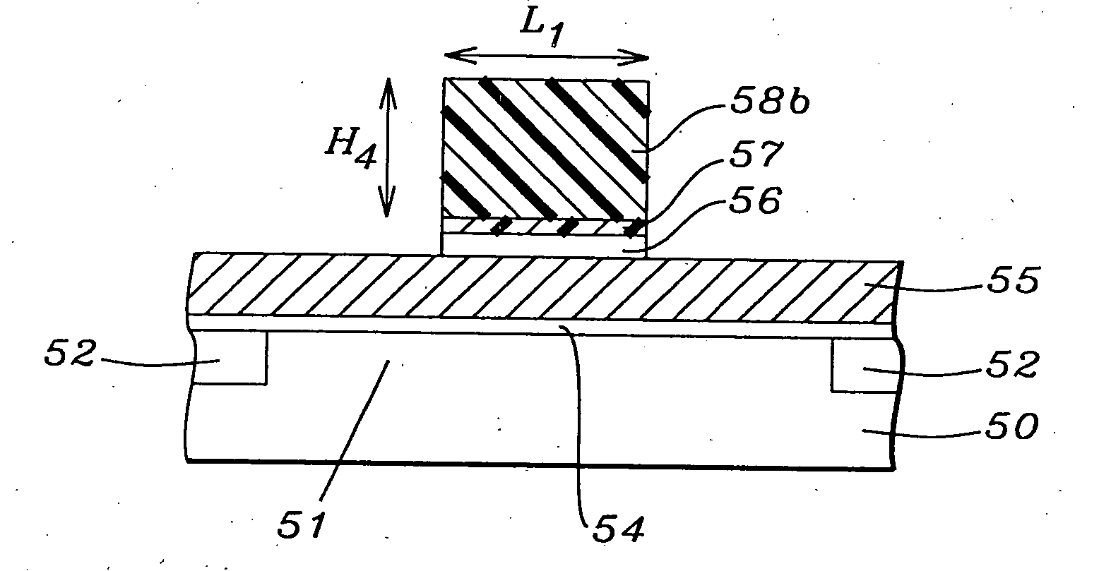
[0029] The first embodiment is illustrated in FIGS. 4a-4d. Referring to FIG. 4a, a substrate 50 that is typically silicon with a field implant of an impurity such as boron is provided and has an active area 51 located between two isolation regions 52. Isolation regions can be formed by a LOCOS method or in this case, shallow trench isolation (STI) features 52 are depicted. The STI regions 52 are filled with an insulating material such as silicon dioxide or a low k dielectric material. A gate dielectric layer 54 is formed on substrate 50 by a method such as chemical vapor deposition (CVD) and is comprised of silicon oxide, silicon nitride, or silicon carbide and has a thickness in the range of about 10 to 30 Angstroms. When gate dielectric layer 54 is silicon oxide, it may also be formed by placing substrate 50 in a thermal oxidation furnace with a dry oxygen ambient at approximately 600° C. to 800° C. Other methods such as RTO (rapid thermal oxidation) may also be used to grow an ox...

second embodiment

[0041] In a second embodiment, the method of the present invention is employed to form shallow trench isolation (STI) features in a substrate. Referring to FIG. 6a, a substrate 60 is provided which typically contains active and passive devices in a substructure (not shown). A silicon nitride layer 61 having a thickness of from 300 to 1000 Angstroms is deposited by a CVD method on the substrate 60. Then a hardmask 62 such as silicon oxynitride with a thickness between 200 and 800 Angstroms is deposited on the nitride layer 61. Optionally, an organic or inorganic ARC (not shown) is deposited on the hardmask to improve process latitude in a later photoresist patterning step.

[0042] A photoresist composition is then spin coated and patterned to form trench openings 64 and 65 that are separated by a photoresist layer 63 having a height H6 of between 1500 and 4000 Angstroms and a width L3. The photoresist composition is selected depending on the desired width L3 or on the width of trenches...


PUM


Abstract

A process is described for transferring a photoresist pattern into a substrate. In one embodiment a stack comprised of a top photoresist layer, a middle ARC layer, and a bottom hardmask is formed over a gate electrode layer. A line in the photoresist pattern is anisotropically transferred through the ARC and hardmask. Then an isotropic etch to trim the linewidth by 0 to 50 nm per edge is performed simultaneously on the photoresist, ARC and hardmask. This method minimizes the amount of line end shortening to less than three times the dimension trimmed from one line edge. Since a majority of the photoresist layer is retained, the starting photoresist thickness can be reduced by 1000 Angstroms or more to increase process window. The pattern is then etched through the underlying layer to form a gate electrode. The method can also be used to form STI features in a substrate.

Description

DOMESTIC PRIORITY CLAIM [0001] This application is a continuation of U.S. patent application Ser. No. 10 / 284,963 filed Oct. 31, 2002, and entitled, “Novel Approach to Improve Line End Shortening,” which is hereby incorporated by reference in its entirety.FIELD OF THE INVENTION [0002] The invention relates to a method of fabricating semiconductor structures, and more particularly, to etch transferring a photoresist pattern into a substrate during the formation of an integrated circuit. BACKGROUND OF THE INVENTION [0003] There is a constant demand to improve the performance of a Metal-oxide-semiconductor field effect transistor (MOSFET) which typically involves faster speeds and higher reliability. The speed of the device is usually governed by the width of the gate electrode that is also referred to as the gate length and which is typically one of the smallest dimensions in the device. The critical dimension (CD) or gate length is being reduced in each successive technology generatio...

Claims


Application Information

Patent Timeline
Patent Type & Authority Applications(United States)
IPC IPC(8): H01L21/033H01L21/28H01L21/308H01L21/311H01L21/3213
CPCH01L21/0337H01L21/0338H01L21/28123H01L21/3081Y10S430/151H01L21/3088H01L21/31116H01L21/32139H01L21/3086
Inventor HUANG, MING-JIETAO, HUN-JAN
Owner TAIWAN SEMICON MFG CO LTD
Why Eureka
Try Eureka