Reflection type mask blank and reflection type mask and production methods for them

a reflection mask and mask blank technology, applied in the field of reflection masks and reflective mask blanks, can solve the problems of insufficient contrast upon inspection, insufficient detection of pattern defects, inaccurate inspection of defects, etc., and achieve the effect of accurate and rapid inspection

Active Publication Date: 2005-09-22
PANASONIC CORP +1
View PDF2 Cites 110 Cited by
  • Summary
  • Abstract
  • Description
  • Claims
  • Application Information

AI Technical Summary

Benefits of technology

[0023] It is an object of this invention to provide a reflective mask and a reflective mask blank which enable mask pattern inspection to be accurately and quickly carried out and to provide methods of producing the mask and the mask blank.

Problems solved by technology

Therefore, if the difference in reflectivity for the wavelength of the inspection light between the surface of the buffer layer and the surface of the absorber layer is small, a contrast upon the inspection is insufficient so that defect inspection can not accurately be carried out.
For the inspection light having a wavelength of 257 nm, the difference between the reflectivity of the surface of the absorber and the reflectivity on the surface of the buffer layer is small so that the contrast upon the inspection is insufficient.
As a result, a pattern defect can not sufficiently be detected during the inspection of the mask and an accurate defect test can not be carried out.
On the other hand, by inspection with an electron microscope using an electron beam, an EUV absorber film is damaged by the electron beam irradiated thereto.
Therefore, practical use is difficult.
However, in order to equip the inspection apparatus with an EUV light source, an extremely high facility cost is required.
Further, as compared with an existing inspection apparatus using an ultraviolet wavelength, a pattern inspecting step is increased in scale and complicated because a structure of holding a whole of an optical system in vacuum is required in order to avoid absorption in atmospheric air.
Therefore, if the difference in reflectivity between the surface of the buffer layer 13 and the surface of the absorber layer 14 for the wavelength of the inspection light is small, the contrast during the first inspection is inferior so that the first inspection can not accurately be carried out.
If the difference in reflectivity between the surface of the multilayer reflective film and the surface of the absorber layer for the wavelength of the inspection light is small, the contrast during the final inspection is inferior so that the final inspection can not accurately be carried out.
Therefore, the difference in reflectivity is small so that a sufficient contrast can not be obtained in the pattern inspection.
In this case, it is also difficult to achieve a contrast sufficient to obtain an accurate result in the inspection for final confirmation.
In this case, however, edge roughness after pattern formation is increased so that the dimensional accuracy of the mask is degraded.
In this case also, the edge roughness after pattern formation is increased and the dimensional accuracy of the mask is degraded.

Method used


Image

  • Reflection type mask blank and reflection type mask and production methods for them
  • Reflection type mask blank and reflection type mask and production methods for them
  • Reflection type mask blank and reflection type mask and production methods for them

Examples


first embodiment

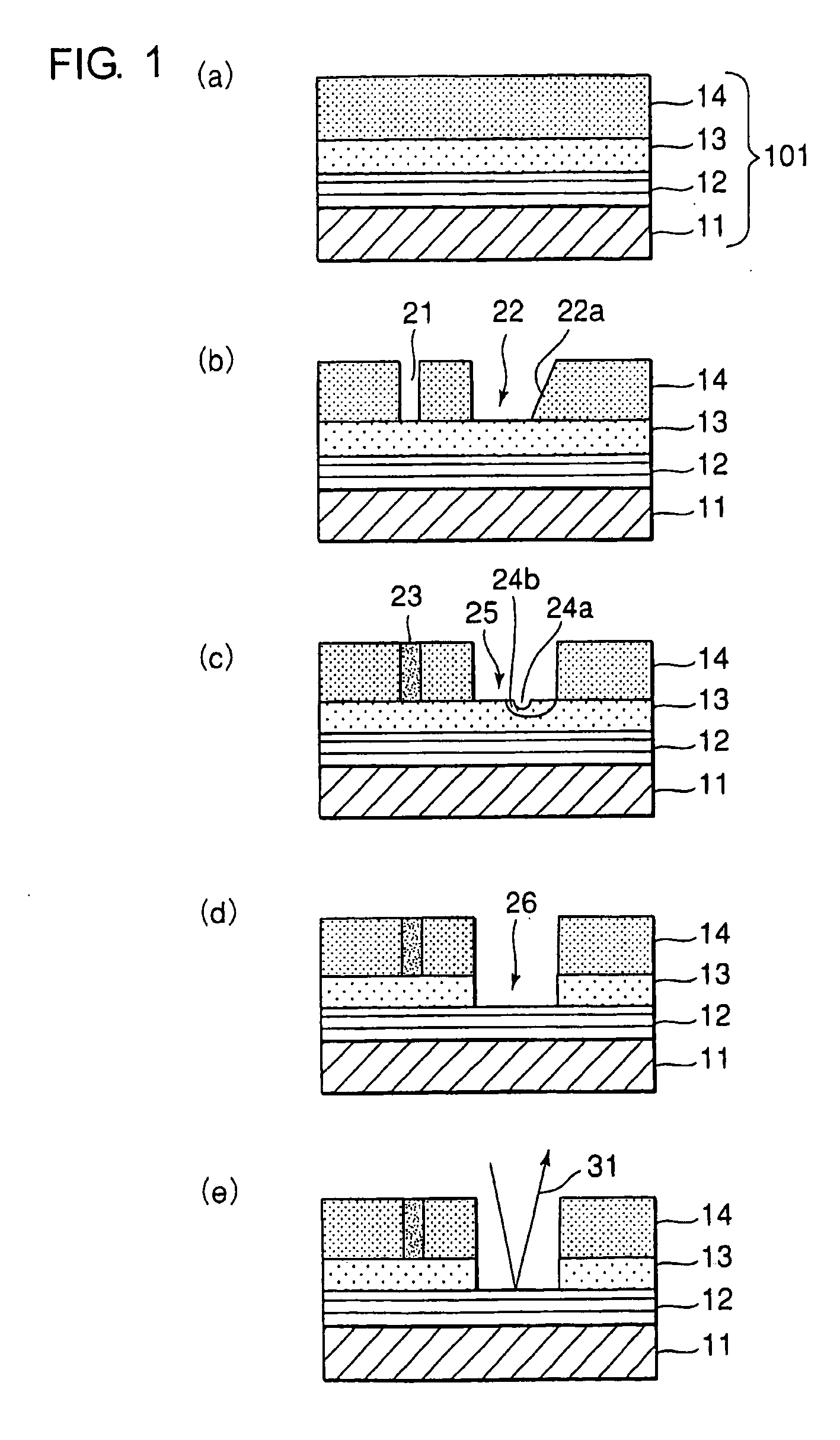
[0062] Now, a first embodiment of this invention will be described in detail with reference to the drawing.

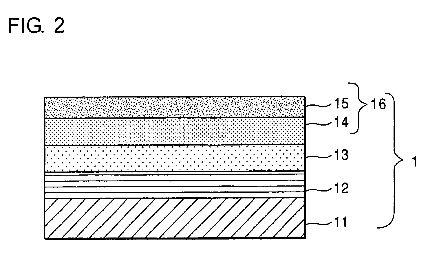
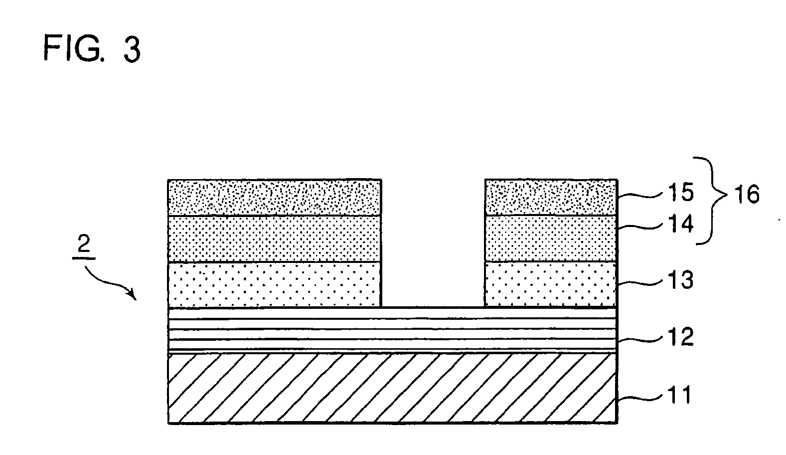
[0063]FIG. 2 is a schematic sectional view of a mask blank according to the first embodiment of this invention and FIG. 3 is a schematic sectional view of a reflective mask formed by using the mask blank in FIG. 2.

[0064] The mask blank according to the first embodiment of this invention has a structure illustrated in FIG. 2. Specifically, the mask blank 1 comprises a substrate 11 on which a reflective layer 12 for reflecting exposure light in a short-wavelength region including an EUV region, a buffer layer 13 for protecting the reflective layer 12 during formation of a mask pattern, and an absorber layer 16 for absorbing the exposure light are successively formed. In this embodiment, the absorber layer 16 has a two-layer structure comprising as a lower layer an exposure light absorbing layer 14 formed by an absorber for the exposure light in the short-wavelength region inclu...

example 1-1

[0143] The respective layers were deposited on the substrate 11 to produce a mask blank. Herein, a low-expansion SiO2—TiO2 glass substrate having an outer dimension of 6 inch square and a thickness of 6.3 mm was used as the substrate 11. The glass substrate was subjected to mechanical polishing to have a smooth surface of 0.12 nmRms (Rms: root mean square roughness) and a flatness of 100 nm or less.

[0144] At first, on the substrate 11, a Mo / Si laminate film of molybdenum (Mo) and silicon (Si) was deposited by DC magnetron sputtering as the EUV light reflective layer 12. At first, using a Si target, a Si film was deposited to 4.2 nm under an Ar gas pressure of 0.1 Pa. Then, using a Mo target, a Mo film was deposited to 2.8 nm under an Ar gas pressure of 0.1 Pa. Defining the above-mentioned deposition as one period, 40 periods of deposition was carried out. Finally, a Si film was deposited to 7 nm. The total thickness was 287 nm. The multilayer reflective film thus obtained had a ref...

example 1-2

[0163] In the manner similar to Example 1-1, a Mo / Si laminate film of molybdenum (Mo) and silicon (Si) was deposited on the substrate 11 as the EUV light reflective layer 12. On the reflective layer, a SiO2 thin film was deposited to a thickness of 50 nm as the buffer layer 13.

[0164] On the buffer layer, a tantalum (Ta) thin film was formed to a thickness of 50 nm as the exposure light absorbing layer (comprising the EUV light absorber) 14. Specifically, using a Ta target, deposition was carried out by DC magnetron reactive sputtering using an argon gas.

[0165] On the exposure light absorbing layer, a TaO thin film was deposited to a thickness of 10 nm as the low-reflectivity layer 15 for the inspection light having a wavelength of 257 nm. Specifically, using the same Ta target and in the same deposition chamber as those in the formation of the lower layer of Ta, deposition was carried out by DC magnetron reactive sputtering using a mixed gas of argon and oxygen. The film had a com...


PUM

PropertyMeasurementUnit
reflectivityaaaaaaaaaa
thicknessaaaaaaaaaa
wavelengthaaaaaaaaaa

Abstract

A reflective mask blank has a substrate (11) on which a reflective layer (12) for reflecting exposure light in a short-wavelength region including an extreme ultraviolet region and an absorber layer (16) for absorbing the exposure light are successively formed. The absorber layer (16) has an at least two-layer structure including as a lower layer an exposure light absorbing layer (14) formed by an absorber for the exposure light in the short-wavelength region including the extreme ultraviolet region and as an upper layer a low-reflectivity layer (15) formed by an absorber for inspection light used in inspection of a mask pattern. The upper layer is made of a material containing tantalum (Ta), boron (B), and nitrogen (N). The content of B is 5 at % to 30 at %. The ratio of Ta and N (Ta:N) falls within a range of 8:1 to 2:7. Alternatively, the reflective mask blank has a substrate on which a multilayer reflective film and an absorber layer are successively formed. In this case, the absorber layer is made of a material containing tantalum (Ta), boron (B), and nitrogen (N). The content of B is 5 at % to 25 at %. The ratio of Ta and N (Ta:N) falls within a range of 8:1 to 2:7.

Description

TECHNICAL FIELD [0001] This invention relates to a reflective mask and a reflective mask blank suitably used in lithography using exposure light within a short-wavelength region, such as extreme ultraviolet light, and to methods of producing the mask and the mask blank and, in particular, to a reflective mask and the like enabling accurate and quick inspection of a mask pattern. BACKGROUND ART [0002] In recent years, following the development of a highly-integrated semiconductor product, such as a semiconductor memory and a VLSI (Very Large Scale Integrated circuit), there arises a demand for a fine pattern exceeding a transfer limit in photolithography. In order to enable such a fine pattern to be transferred, proposal has been made of lithography using extreme ultraviolet light (hereinafter abbreviated to EUV light) having a shorter wavelength or the like. It is noted here that the EUV light means light of a wavelength band within a soft X-ray region or a vacuum ultraviolet region...

Claims


Application Information

Patent Timeline
Patent Type & Authority Applications(United States)
IPC IPC(8): G03F1/52G03F1/00G03F1/50H01L21/027
CPCB82Y10/00B82Y40/00G03F1/74G03F1/58G03F1/24Y10T428/31616G03F1/52G03F7/18G03F7/091H01L21/0276
Inventor ISHIBASHI, SHINICHISHOKI, TSUTOMUHOSOYA, MORIOSHIOTA, YUKIKUREISHI, MITSUHIRO
Owner PANASONIC CORP
Why Eureka
Try Eureka